
075582814553

A buck regulator IC is used when a circuit needs a lower, stable DC voltage from a higher input voltage. It is widely used because many electronic devices cannot run directly from batteries, adapters, or industrial power rails without proper voltage regulation. Unlike linear regulators that waste extra voltage as heat, buck regulators use fast switching, an inductor, and capacitors to convert power more efficiently. This article explains how buck regulator ICs work, the difference between synchronous and non-synchronous types, popular buck regulator IC families, and the key factors to consider when choosing the right device for a design.
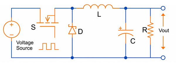
Buck regulator IC is a switching voltage regulator that reduces a higher DC input voltage to a lower DC output voltage while maintaining high efficiency. Unlike linear regulators, which dissipate excess voltage as heat, buck regulators use high-speed switching and energy storage components to transfer power more efficiently.As shown in figure above, the circuit consists of a switch (S), diode (D), inductor (L), capacitor (C), and load resistor (R). These components work together to convert the input voltage into a stable lower output voltage (Vout).
When the switch (S) turns on, current flows from the voltage source through the inductor (L) and into the load (R). During this period, the inductor stores energy in its magnetic field while simultaneously supplying power to the load. The capacitor (C) also charges and helps maintain a stable output voltage.When the switch turns off, the magnetic field in the inductor begins to collapse. The stored energy in the inductor keeps current flowing through the circuit by providing an alternate current path through the diode (D). This allows power to continue reaching the load even when the switch is not conducting.
The capacitor (C) filters voltage fluctuations caused by the switching action and helps reduce output ripple. Meanwhile, the inductor (L) smooths the current flow, preventing sudden current changes. Together, the inductor and capacitor form a filter that produces a steady DC output voltage.The buck regulator controls the output voltage by adjusting the switch's duty cycle, which is the ratio of on-time to the total switching period. A longer on-time generally results in a higher output voltage, while a shorter on-time produces a lower output voltage. By continuously monitoring and adjusting the switching operation, the buck regulator maintains a stable and efficient output voltage for the connected load.
Buck regulators can be divided into two main types: synchronous and non-synchronous buck regulators. The main difference is the component used to carry the inductor current when the main switching transistor turns off.
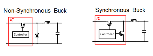
The non-synchronous buck regulator uses a diode as the freewheeling path. When the main switch inside the IC turns off, the inductor still needs a path to keep current flowing. The diode conducts this current and allows the stored energy in the inductor to continue supplying the load.
This design is simple, low-cost, and easy to use. However, the diode has a forward voltage drop, which causes extra power loss. Because of this, non-synchronous buck regulators usually have lower efficiency and generate more heat, especially when the output current is high.
In the synchronous buck regulator shown in the same figure, the diode is replaced by a second MOSFET inside the IC. When the main MOSFET turns off, the lower MOSFET turns on and provides a low-resistance path for the inductor current. This reduces conduction loss and improves efficiency.
Synchronous buck regulators are commonly used in modern circuits that need high efficiency, such as processors, FPGAs, graphics cards, servers, battery-powered devices, and communication equipment. They are better for low-output-voltage and high-current designs because they waste less power as heat.
However, synchronous buck regulators are usually more complex and may cost more than non-synchronous types. The controller must carefully manage the timing of the two MOSFETs to avoid shoot-through current. Even with this added complexity, synchronous designs are often preferred in modern power supplies because they provide better efficiency and thermal performance.
The TPS62130A is one of the most popular synchronous buck regulator ICs. It has a relatively high output current capability of up to 3A. The device operates from a wide 3V to 17V input range, allowing it to support both battery-powered and fixed-supply applications. In the pinout, PVIN (Pins 11–12) and AVIN (Pin 10) receive the input voltage, while the SW pins (Pins 1–3) connect to the external inductor for energy transfer. FB (Pin 5) monitors the output voltage for regulation, EN (Pin 13) enables or disables the converter, PG (Pin 4) provides a power-good status signal, and SS/TR (Pin 9) controls soft-start timing to reduce startup stress.
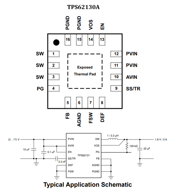
Referring to the typical application circuit, the TPS62130A converts an input voltage between 3V and 17V into a stable 1.8V output at up to 3A. When the internal switching MOSFETs operate, energy is transferred through the external inductor connected to the SW pin. The output capacitors smooth the switching waveform into a stable DC voltage, while the feedback network connected to the FB pin continuously measures the output and adjusts the switching duty cycle to maintain regulation. The 100 kΩ resistor connected to the PG pin creates a power-good signal that indicates when the output voltage is within the proper operating range. Because the TPS62130A uses a synchronous architecture with integrated MOSFETs, it achieves high efficiency, reduces heat generation, and minimizes the number of external components required, making it a popular choice for modern compact power supply designs.
The TPS54302 is a highly popular synchronous buck regulator from Texas Instruments. It provides up to 3A output current, supports a wide 4.5V to 28V input range, and requires only a few external components. Its small 6-pin SOT-23 package makes it attractive for space-constrained products such as industrial controllers, set-top boxes, audio equipment, printers, embedded systems, and 12V/24V power distribution applications. In the pinout, VIN (Pin 3) receives the input supply, SW (Pin 2) connects to the external inductor and serves as the switching node, FB (Pin 4) monitors the output voltage through a resistor divider, EN (Pin 5) enables or disables the regulator, BOOT (Pin 6) drives the internal high-side MOSFET, and GND (Pin 1) provides the ground reference. The device integrates both switching MOSFETs internally, reducing component count while maintaining high efficiency.
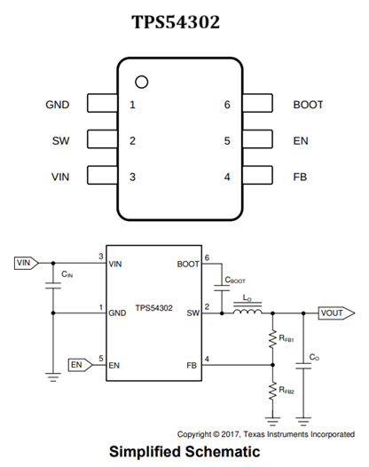
In the simplified application circuit above, the input voltage is applied to the VIN pin and filtered by the input capacitor (CIN). The TPS54302 then switches the internal MOSFETs at a fixed frequency of approximately 400 kHz, generating a pulsed waveform at the SW pin. This switching energy passes through the external inductor (LO) and output capacitor (CO) to produce a smooth DC output voltage. The resistor divider (RFB1 and RFB2) feeds a scaled version of the output voltage back to the FB pin, allowing the IC to continuously adjust its duty cycle and maintain stable regulation. The BOOT capacitor (CBOOT) supplies the gate-drive voltage needed for the high-side MOSFET, while the EN pin allows external control of startup and shutdown.
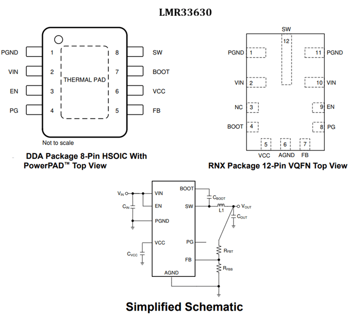
The LMR33630 supports a wide 3.8V to 36V input range, delivers up to 3A output current, and is suitable for industrial systems, telecom equipment, sensors, PLCs, and 24V power rails. Referring to the pinout, VIN receives the input supply, SW connects to the external inductor, FB senses the output voltage through a resistor divider, EN controls startup, BOOT drives the high-side MOSFET, PG gives a power-good signal, and PGND/AGND separate power and signal grounds for better noise performance. In the simplified circuit, the input capacitor filters the supply, the IC switches current through the SW pin, the inductor and output capacitor smooth it into a stable DC output, and the feedback resistors help the regulator adjust its duty cycle to maintain the required voltage. Because it combines integrated MOSFETs, high efficiency, low EMI performance, thermal pad support, and simple external circuitry, the LMR33630 is widely used in compact and reliable power supply designs.
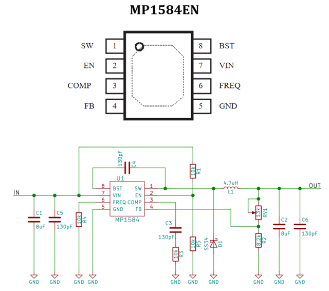
The MP1584EN can provide up to 3A output current from a wide 4.5V to 28V input range. In the pinout, VIN receives the input supply, SW connects to the external inductor, FB senses the output voltage, EN controls on/off operation, BST supports high-side switch driving, FREQ adjusts switching frequency, COMP stabilizes regulation, and GND is the ground reference. In the application circuit, the input capacitors filter the supply, the IC switches current through the SW pin, the 4.7µH inductor and output capacitors smooth the pulsed signal into DC output, and the feedback resistors plus variable resistor adjust and regulate the output voltage.
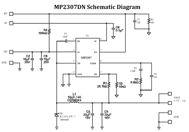
The MP2307DN is a widely used synchronous buck regulator IC known for its low cost, high efficiency, and ability to deliver up to 3A output current from a wide 4.75V to 23V input range. It is commonly found in DC-DC converter modules, embedded systems, Arduino projects, industrial control boards, and consumer electronics. Referring to the schematic, VIN receives the input voltage, SW connects to the external inductor (L1) for power conversion, FB monitors the output voltage through the resistor divider network (R1 and R3), COMP is used for loop compensation and stability, EN enables or disables the regulator, SS controls the soft-start function to reduce inrush current during startup, BS drives the internal high-side MOSFET, and GND provides the ground reference.
During operation, the IC switches the internal MOSFETs, transferring energy through the inductor and output capacitors (C5 and C9) to generate a stable 3.3V/3A output. The feedback circuit continuously monitors the output voltage and adjusts the switching duty cycle as needed to maintain regulation.
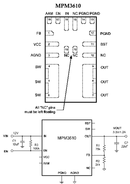
The MPM3610 is a highly integrated power module from Monolithic Power Systems that combines a synchronous buck regulator, power MOSFETs, inductor, and control circuitry into a single compact package. It operates from a wide input voltage range and can deliver up to 1.2A output current with very few external components. Referring to the pinout, IN receives the input supply voltage, OUT provides the regulated output, FB monitors the output voltage through the resistor divider network, EN controls startup and shutdown, BST supports the internal high-side switch driver, SW is the internal switching node, VCC powers the internal control circuitry, while PGND and AGND provide separate power and analog grounds for improved noise performance. In the application circuit, a 12V input is converted into a stable 3.3V output at 1.2A, with the feedback resistors (R1 and R2) setting the output voltage and the output capacitor (C2) reducing ripple.
The LTC3639 is a unique high-voltage synchronous buck regulator from Analog Devices. It is designed for applications requiring direct conversion from high DC voltages. Its most notable feature is its exceptionally wide 5V to 150V input voltage range, allowing it to operate directly from industrial power supplies, telecom systems, automotive equipment, and high-voltage control circuits without additional pre-regulation stages.
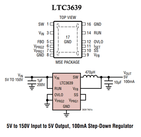
Referring to the pinout, VIN receives the input voltage, SW connects to the external inductor, VFB monitors the output voltage, RUN enables or disables the regulator, SS controls soft-start behavior, ISET sets the peak current limit, OVLO provides overvoltage lockout protection, and VPRG1/VPRG2 are used for operating mode configuration.
In the application circuit, the LTC3639 converts an input voltage ranging from 5V to 150V into a regulated 5V output at 100mA. The switching action at the SW pin transfers energy through the 470µH inductor, while the output capacitor smooths the voltage and the VFB pin continuously monitors the output to maintain regulation. Because it can handle extremely high input voltages while requiring relatively few external components, the LTC3639 is a popular choice for industrial, instrumentation, smart-metering, and high-voltage power conversion applications.
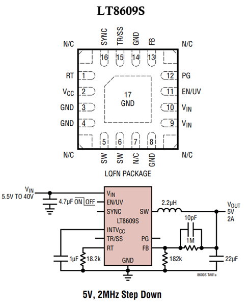
The LT8609S is widely used in automotive, industrial, telecommunications, and embedded power systems because it combines high efficiency, low EMI operation, and a wide 3V to 42V input voltage range. It can deliver up to 2A output current while operating at switching frequencies as high as 2MHz, allowing designers to use smaller inductors and capacitors for compact power supplies. Referring to the pinout, VIN (Pins 9 and 10) receives the input voltage, SW (Pins 5 and 6) connects to the external inductor, FB (Pin 13) monitors the output voltage through a feedback network, EN/UV (Pin 11) controls enable and undervoltage lockout functions, PG (Pin 12) provides a power-good signal, RT (Pin 1) sets the switching frequency, TR/SS (Pin 15) controls soft-start behavior, and SYNC (Pin 16) allows synchronization with an external clock.
In the application circuit, the LT8609S converts an input voltage from 5.5V to 40V into a regulated 5V, 2A output, with the inductor and output capacitors filtering the switching waveform into a stable DC voltage while the feedback divider continuously adjusts the duty cycle to maintain regulation. Thanks to its Silent Switcher® architecture, excellent efficiency, compact design, and low electromagnetic interference, the LT8609S is a popular choice for noise-sensitive and space-constrained power applications.
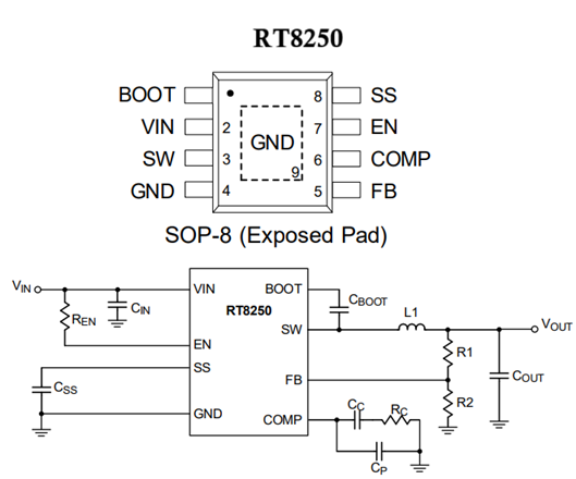
The RT8250 is designed for efficient step-down power conversion in consumer electronics, networking equipment, industrial controls, and embedded systems. It supports a wide input voltage range and can deliver up to 3A output current, making it suitable for powering processors, communication modules, and digital circuits. Referring to the pinout, VIN (Pin 2) receives the input voltage, SW (Pin 3) connects to the external inductor (L1) for energy transfer, FB (Pin 5) monitors the output voltage through the resistor divider (R1 and R2), COMP (Pin 6) is used for loop compensation and stability control, EN (Pin 7) enables or disables the regulator, SS (Pin 8) controls soft-start operation to reduce startup current surge, BOOT (Pin 1) drives the internal high-side MOSFET, and GND (Pin 4) provides the ground reference.
In the application circuit, the RT8250 converts the input voltage into a regulated output by switching current through the inductor and output capacitor network, while the feedback circuit continuously adjusts the switching duty cycle to maintain a stable output voltage. Its integrated MOSFETs, high efficiency, soft-start capability, and low external component count make the RT8250 a widely used solution for compact and reliable DC-DC power supply designs.
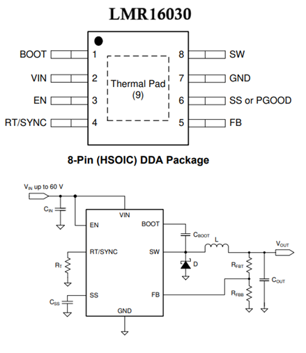
The LMR16030 is a popular non-synchronous buck regulator from Texas Instruments. Good for industrial, automotive, consumer, and distributed power supply applications requiring high input voltage capability. It supports an input voltage range of up to 60V and can deliver up to 3A output current, making it suitable for 24V and 48V power systems, industrial controllers, sensors, and communication equipment. Referring to the pinout, VIN (Pin 2) receives the input voltage, SW (Pin 8) connects to the external inductor and switching node, FB (Pin 5) monitors the output voltage through the feedback resistor divider, EN (Pin 3) controls startup and shutdown, RT/SYNC (Pin 4) sets the switching frequency or allows synchronization to an external clock, SS/PGOOD (Pin 6) provides soft-start or power-good functionality depending on the device version, BOOT (Pin 1) drives the internal high-side MOSFET, and GND (Pin 7) serves as the ground reference.
In the application circuit, the input voltage is filtered by the input capacitor, switched through the SW pin, and transferred through the external inductor and output capacitor to generate a stable DC output voltage, while the feedback network continuously adjusts the duty cycle to maintain regulation. Its ability to operate directly from high-voltage inputs, combined with good efficiency, robust protection features, and a simple external component count, has made the LMR16030 a widely used buck regulator in industrial and high-voltage power conversion designs.
• Determine the Input Voltage Range - Choose a buck regulator that supports the highest and lowest input voltages expected in your application.
• Calculate the Required Output Voltage - Ensure the regulator can provide the exact output voltage needed by the load, either fixed or adjustable.
• Check the Output Current Requirement - Select an IC with a current rating higher than the maximum load current to provide sufficient design margin.
• Consider Efficiency Requirements - Higher-efficiency regulators reduce power loss, heat generation, and energy consumption.
• Evaluate Switching Frequency - Higher switching frequencies allow smaller inductors and capacitors but may increase switching losses.
• Review Thermal Performance - Check power dissipation, thermal resistance, and cooling requirements, especially for high-current applications.
• Verify Protection Features - Look for overcurrent, overvoltage, thermal shutdown, short-circuit, and undervoltage lockout protection.
• Consider Package Size and PCB Space - Select a package that fits the available board area and thermal design constraints.
• Check External Component Requirements - Some regulators require only a few capacitors, while others need additional compensation networks and filtering components.
• Evaluate EMI and Noise Performance - Low-EMI regulators are preferred for communication, automotive, RF, and noise-sensitive applications.
• Match the IC to the Application - Low-power IoT devices, industrial equipment, automotive systems, and high-voltage power supplies often have different regulator requirements.
• Consider Future Scalability - Select a regulator that can accommodate possible future increases in power or performance requirements.
• Study the Datasheet and Reference Design - Verify specifications, recommended layouts, application circuits, and design guidelines before final selection.
As shown in the examples, each buck regulator IC has different strengths, such as high current capability, wide input voltage range, low EMI performance, compact packaging, or high-voltage operation. The best choice depends on the input voltage, output voltage, load current, efficiency target, thermal limits, PCB space, noise requirements, and protection features needed by the application. By understanding how these ICs work and comparing their specifications carefully, you can select a buck regulator that provides safe, stable, and efficient power for their circuit.

 FPGA / CPLD
 Memory
 MOS
MOS  MCU
MCU  DSP
DSP OCEP
OCEP Secondary
  Other
Other