
075582814553

Field-Effect Transistors (FETs) are at the center of modern electronics, serving as basic components in everything from microprocessors to power converters. As voltage-controlled, unipolar devices, FETs offer high input impedance, fast switching speeds, and low power consumption, traits that make them requisite in analog, digital, and RF applications. This comprehensive guide explores the working principles, structure, types, electrical characteristics, and diverse applications of FETs, including advanced innovations like FinFETs and GaN FETs. This article will help you understand how FETs shape today’s electronic systems.
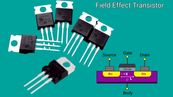
Figure 1. Field-Effect Transistor (FET)
A Field-Effect Transistor (FET) is a voltage-controlled semiconductor device that regulates current flow between two terminal source and drain, by applying a voltage to a third terminal called the gate. Unlike bipolar junction transistors (BJTs), which rely on both electrons and holes, FETs operate with only one type of charge carrier (electrons or holes), making them unipolar devices. This design offers high input impedance and efficient performance, making FETs ideal for many analog and digital applications.
The concept of the FET dates back to the 1920s, attributed to Julius Lilienfeld and later Oskar Heil. However, practical implementation wasn’t realized until 1959, when Mohamed Atalla and Dawon Kahng at Bell Labs introduced the MOSFET (Metal-Oxide-Semiconductor FET). This innovation laid the groundwork for modern integrated circuits and revolutionized the fields of computing and electronics.
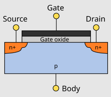
Figure 2. Structure and Terminals of FETs
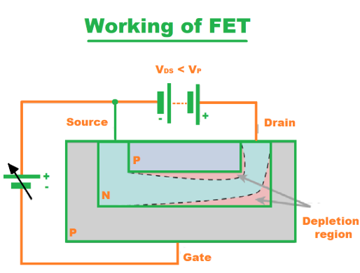
Figure 3. Working of FET
The operation of a Field-Effect Transistor (FET) relies on controlling the flow of current through a semiconductor channel using an electric field generated by the gate terminal. When a voltage is applied to the gate, it creates an electric field that either allows or restricts the movement of charge carriers (electrons or holes) between the source and drain terminals.
The mechanism of control depends on the type of FET:
Enhancement-mode FETs (e.g., most MOSFETs) - These require a gate voltage to create a conductive channel. For example, in an N-channel enhancement-mode MOSFET, applying a positive gate voltage attracts electrons to form a channel, allowing current to flow from drain to source.
Depletion-mode FETs (e.g., some JFETs and MOSFETs) - These have a naturally conductive channel at zero gate voltage. Applying a gate voltage of the appropriate polarity depletes the channel of carriers, reducing or stopping current flow.
In both cases, no significant current flows into the gate, especially in insulated-gate devices like MOSFETs. Instead, the gate voltage simply establishes an electric field, making FETs voltage-controlled rather than current-controlled devices.
This characteristic gives FETs:
1. High input impedance reduces the loading effect on preceding stages
2. Low power consumption, especially in switching applications
3. Fast switching capability, making them ideal for digital logic circuits
Field-Effect Transistors come in several types, each tailored for specific electrical characteristics and application domains. Below are the primary FET types, ranging from basic to advanced variants:
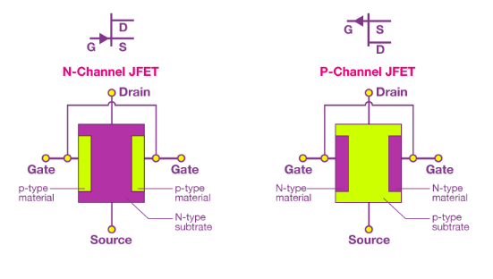
Figure 4. Junction Field-Effect Transistor (JFET)
A JFET controls current using a reverse-bias PN junction between the gate and channel. Applying a negative gate voltage (for N-channel) or positive voltage (for P-channel) expands the depletion region, narrowing the channel and restricting current flow. JFETs operate exclusively in depletion mode, meaning they are normally on when no gate voltage is applied. Their low noise, simple construction, and high input impedance make JFETs ideal for analog circuits, including preamplifiers, voltage buffers, and signal conditioners in audio and instrumentation systems.
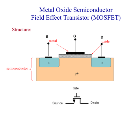
Figure 5. Metal-Oxide-Semiconductor Field-Effect Transistor (MOSFET)
MOSFETs feature a metal gate insulated by a thin oxide layer from the semiconductor channel, resulting in extremely high input impedance and minimal gate current. It has two types:
• Enhancement-mode MOSFETs: These are normally off and require a gate voltage to induce a conductive channel. They dominate digital logic and switching applications.
• Depletion-mode MOSFETs: These are normally off and conduct without gate bias. A gate voltage is applied to reduce or stop current flow.
Due to their high switching speed, low gate drive requirements, and scalability, MOSFETs are used extensively in digital integrated circuits (CMOS), power supplies, motor drivers, and voltage regulators.
These are specialized FET designs developed to meet the demands of modern high-performance electronics:
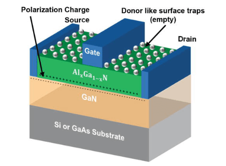
Figure 6. HEMT (High Electron Mobility Transistor)
• HEMT (High Electron Mobility Transistor): Made from compound semiconductors like GaAs or GaN, HEMTs offer extremely fast switching and high-frequency performance. Widely used in RF, microwave, and satellite communication systems.
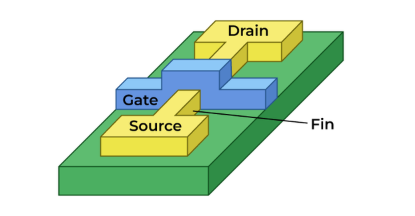
Figure 7. FinFET (Fin Field-Effect Transistor)
• FinFET (Fin Field-Effect Transistor): A 3D structure where the channel resembles a fin protruding from the substrate. Used in advanced microprocessors and SoCs, FinFETs reduce leakage and improve control at nanoscale geometries.
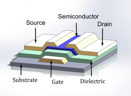
Figure 8. TFT (Thin-Film Transistor)
• TFT (Thin-Film Transistor): Built on insulating substrates like glass or plastic, TFTs are used in LCD panels, e-paper, and flexible electronics, allowing pixel-level switching.
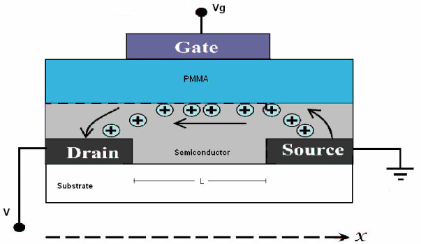
Figure 9. OFET (Organic Field-Effect Transistor)
• OFET (Organic Field-Effect Transistor): Constructed from organic semiconductors, OFETs are promising for low-cost, flexible, and printable electronics, including wearables, smart packaging, and disposable sensors.
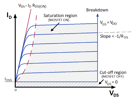
Figure 10. FET Operating Regions
FETs exhibit different behaviors depending on the voltages applied to their terminals, especially the gate-to-source voltage (VGS) and drain-to-source voltage (VDS). These conditions define the FET’s operating region, which determines how the device functions in a circuit, either as a switch or an amplifier.
• Cutoff Region (VGS < Vth): In this region, the gate voltage is below the threshold voltage. No conductive channel is formed, and the FET is turned off, allowing no current (ID) to flow between the drain and the source. This mode is used for digital switching applications where the FET acts as an open circuit.
• Linear or Ohmic Region (VDS < VGS – Vth): Here, the FET operates like a voltage-controlled resistor. A conductive channel forms, and increasing VDS causes a nearly proportional increase in drain current (ID). This region is commonly used for analog switches, variable resistors, and low-dropout regulators.
• Saturation or Active Region (VDS≥ VGS– Vth): The channel is pinched off near the drain, but current continues to flow due to carrier drift. In this mode, ID becomes mostly independent of VDS and is instead governed by VGS, making this region ideal for amplification. Widely used in analog circuits, such as gain stages in amplifiers.
| Parameter | Description |
| Vt (Threshold Voltage) | This is the minimum gate-to-source voltage required to create a conductive channel between the source and drain in enhancement-mode FETs. If VGS is below Vth, the FET remains off. The threshold voltage is used for determining the operating point and logic-level compatibility in digital applications. |
| ID (Drain Current) | Represents the current flowing from the drain to the source terminal when the FET is on. It is influenced by gate voltage, drain-source voltage, and FET dimensions. In amplification, ID varies linearly or nonlinearly depending on the operating region. |
| gm (Transconductance) | Defined as the rate of change of the drain current for the gate voltage (∂ID/∂VGS), transconductance reflects how effectively the gate controls the drain current. Higher gm means stronger amplification capability, making it a critical parameter in analog design. |
| Ciss (Input Capacitance) | Comprises the sum of gate-to-source (Cgs) and gate-to-drain (Cgd) capacitances. It affects how quickly the gate can charge and discharge, impacting switching speed, especially in high-frequency or fast digital circuits. Lower Ciss improves switching performance. |
| Gate Leakage Current (IGSS) | Ideally, the gate of a MOSFET should draw no DC due to its insulated oxide layer. However, minimal leakage current can occur due to imperfections or high-temperature operation. Low gate leakage is used for low-power and battery-operated applications to maintain energy efficiency. |
• High Input Impedance: FETs, especially MOSFETs, exhibit extremely high input impedance, often in the megaohm to gigaohm range. This minimizes the current drawn from the preceding circuit stage, making them ideal for signal buffering, sensor interfaces, and low-noise amplifiers.
• Low Power Consumption: Because the gate of a MOSFET is insulated, it draws virtually no steady-state current. This allows FETs to consume significantly less power than bipolar junction transistors (BJTs), making them highly suitable for battery-powered and energy-efficient systems.
• Thermal Stability: FETs generally exhibit better thermal performance than BJTs. As temperature increases, drain current tends to decrease slightly (negative temperature coefficient), reducing the risk of thermal runaway. This makes them more stable in varying environmental conditions.
• Fast Switching Speeds: Due to their low gate capacitance and the absence of minority carrier storage, MOSFETs can switch on and off rapidly. This characteristic helps in digital logic gates, pulse-width modulation (PWM) systems, and high-frequency switching power supplies.
• Scalability and Integration: FETs are the initial devices in CMOS (Complementary MOS) technology, which enables the creation of VLSI (Very-Large-Scale Integration) circuits found in modern processors, memory chips, and microcontrollers. Their small size and ease of fabrication make them ideal for high-density integration.
• Electrostatic Discharge (ESD) Sensitivity: The very high input impedance of FETs makes the gate terminal particularly vulnerable to electrostatic discharge. A static spark can easily destroy the thin gate oxide in MOSFETs, necessitating careful ESD protection during handling and manufacturing.
• Threshold Voltage Drift: Over time or with exposure to high temperatures and stress, the threshold voltage (Vth) of a FET may shift. This can alter the switching characteristics or biasing points in analog circuits, affecting long-term reliability and precision applications.
• Voltage Limitations: FETs must be operated within their specified maximum voltage ratings (VGS, VDS, etc.). Exceeding these limits can cause oxide breakdown, punch-through, or permanent device failure, especially in high-voltage or inductive load environments.
Field-Effect Transistors (FETs) are widely used in modern electronics due to their high input impedance, low power consumption, fast switching capabilities, and scalability. Their applications span from low-power analog circuits to high-performance digital systems and RF communication.
• Voltage Amplifiers: JFETs and MOSFETs are commonly used in amplifier stages due to their low noise and high gain properties, ideal for audio and instrumentation systems.
• Buffer Circuits: FETs function as voltage followers or source followers to prevent signal loading between stages.
• Analog Switches: MOSFETs can act as precise analog switches in sample-and-hold, multiplexing, and chopper circuits.
• Current Limiters: FETs are used in current regulation circuits, particularly in battery-powered or portable devices.
• CMOS Logic Gates: Complementary MOSFETs (NMOS + PMOS) are the building blocks of CMOS logic used in microprocessors, memory, and digital ICs.
• Level Shifters: FETs help interface logic devices operating at different voltage levels.
• Digital Signal Switching: Used in selectors, bus drivers, and enable/disable control circuits.
• DC-DC Converters: Power MOSFETs serve as efficient switches in buck, boost, and flyback converters.
• Motor Drivers: FETs are used in H-bridge configurations to drive DC motors and stepper motors.
• Inverters and UPS Systems: High-voltage MOSFETs are used in power conversion systems for renewable energy and uninterruptible power supplies.
• Battery Management Systems (BMS): FETs are key elements in overcurrent, overvoltage, and thermal protection in BMS designs.
• Low-Noise Amplifiers (LNAs): MESFETs and HEMTs are favored in RF front-ends due to their superior noise performance.
• Oscillators and Mixers: FETs are integral in high-frequency oscillation and signal mixing applications in communication systems.
• RF Switches and Attenuators: PINFETs are used for signal routing and amplitude control in microwave instruments.
• Flexible and Printed Electronics: Organic FETs (OFETs) are used in e-paper, RFID tags, and flexible display backplanes.
• Medical Electronics: Used in bio-signal acquisition circuits such as ECG, EEG, and implantable devices.
• Sensor Interfaces: FETs are found in gas sensors, pressure sensors, and biosensors, often as impedance buffers or threshold detectors.
• Quantum and Cryogenic Systems: Specialized FETs operate in extremely low temperatures for quantum computing and deep space sensors.
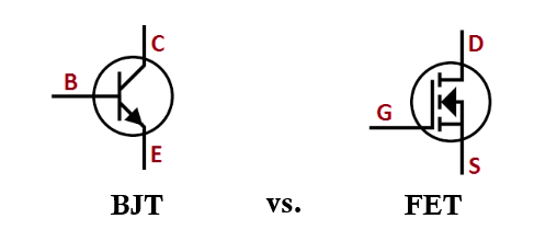
Figure 11. FET and BJT
| Feature | FET (Field-Effect Transistor) | BJT (Bipolar Junction Transistor) |
| Control Type | Voltage-controlled device; the gate voltage modulates the current between source and drain, requiring virtually no gate current in steady state. | Current-controlled device; requires a continuous base current to regulate the collector-emitter current flow. |
| Input Impedance | Extremely high (especially in MOSFETs), often in the megaohm to gigaohm range, minimizing the load on preceding circuit stages. | Low to moderate, typically in the kilohm range, which can load down signal sources and require buffering in high-impedance circuits. |
| Power Consumption | Very low quiescent power since there’s minimal gate current draw. Ideal for battery-powered and energy-efficient systems. | Consumes more power due to continuous base current requirement. Power loss in biasing resistors is also common. |
| Switching Speed | Fast switching, especially in MOSFETs, is 0due to small gate charge. Suitable for high-speed digital logic and power conversion applications. | Slower compared to FETs, limited by minority carrier storage and base charge removal during switching transitions. |
| Noise Performance | Excellent in low-noise applications (JFETs are especially quiet), making them ideal for preamplifiers and sensitive analog front ends. | BJTs can introduce more noise, especially at high gain levels or under poorly biased conditions. |
| Thermal Stability | Good thermal stability due to positive temperature coefficient (in MOSFETs, helpful in parallel operation). | Thermal runaway can occur if not properly managed, due to the negative temperature coefficient of the base-emitter junction. |
| Gain Characteristics | Gain is typically lower and more stable, often defined by external components. | Higher intrinsic current gain (β), which varies significantly with temperature and manufacturing variations. |
| Linearity | Generally, more linear in analog applications when properly biased, especially JFETs and depletion-mode MOSFETs. | It can provide good linearity in small-signal applications, but distortion can be higher without proper biasing and feedback. |
| Applications | Widely used in digital ICs (CMOS), RF amplifiers, power electronics, analog switches, and low-noise amplifiers. | Common in analog circuits like audio amplifiers, linear regulators, switching circuits, and discrete signal processing stages. |
Field-Effect Transistor (FET) technology continues to evolve rapidly, driven by the demand for faster, smaller, and more energy-efficient electronic systems. Innovations in materials, structure, and fabrication techniques are expanding FET capabilities beyond traditional silicon-based designs. Key advancements include:
Silicon Carbide (SiC) and Gallium Nitride (GaN) FETs are revolutionizing power electronics by enabling high-voltage and high-frequency operation with superior thermal performance and lower switching losses. These materials offer higher breakdown voltages, faster switching speeds, and greater efficiency compared to traditional silicon. Applications include electric vehicles (EVs), solar inverters, high-efficiency power supplies, and 5G RF amplifiers.
FinFETs represent a major leap in transistor design for advanced CMOS technology nodes (below 16nm). Instead of a flat planar structure, FinFETs use a vertical "fin"-like channel that rises above the substrate, allowing better gate control over the channel and reducing short-channel effects. They are critical to achieving high transistor density, low leakage current, and improved performance in modern CPUs, GPUs, and SoCs used in smartphones and high-performance computing.
Carbon Nanotube FETs use single-walled carbon nanotubes as the channel material, offering exceptional electrical conductivity, mechanical strength, and thermal stability. These transistors have the potential to operate at terahertz speeds while consuming less power, with extremely low leakage current. CNTFETs are still in the research stage but are considered strong candidates for replacing silicon in future nanoelectronics and quantum computing architectures.
Emerging flexible FETs use organic or printed semiconductor materials on plastic substrates, allowing for bendable, lightweight, and low-cost electronics. These are enabling new applications in wearable technology, electronic textiles (e-textiles), foldable displays, biomedical sensors, and flexible IoT devices. Their mechanical flexibility makes them ideal for integration into non-flat surfaces and human-interfacing systems.
Field-Effect Transistors continue to drive technological advancement through their versatility, efficiency, and scalability. From traditional JFETs and MOSFETs to cutting-edge FinFETs and CNTFETs, their roles span across consumer electronics, power systems, telecommunications, and emerging flexible devices. As innovations in materials and design progress, FETs will remain foundational to the next generation of electronic innovation.

 FPGA / CPLD
 Memory
 MOS
MOS  MCU
MCU  DSP
DSP OCEP
OCEP Secondary
  Other
Other