
075582814553

The INA333 instrumentation amplifier IC is designed for accurate measurement of very small differential signals. This article explains the INA333 main features, pin functions, equivalent parts, working principle, proper usage, real-world applications, and comparison with other instrumentation amplifiers.
The AD623
• INA188
| Parameter | INA333 Specification |
| Device Type | Precision Instrumentation Amplifier |
| Supply Voltage Range | 1.8 V to 5.5 V |
| Absolute Maximum Supply Voltage | 7 V |
| Gain Range | 1 to 1000 |
| Gain Formula | G = 1 + (100 kΩ / RG) |
| Input Offset Voltage | 25 μV (Max), G ≥ 100 |
| Offset Voltage Drift | 0.1 μV/°C, G ≥ 100 |
| Input Noise Density | 50 nV/√Hz, G ≥ 100 |
| Common-Mode Rejection Ratio (CMRR) | 100 dB (Min), G ≥ 10 |
| Input Bias Current | 200 pA (Max) |
| Quiescent Current | 50 μA (Typical) |
| Input Voltage Range | (V−) + 0.1 V to (V+) − 0.1 V |
| Output Voltage Range | (V−) + 0.05 V to (V+) − 0.05 V |
| RFI Filtering | Integrated RFI Filtered Inputs |
| Operating Temperature Range | −40°C to +125°C |
| Storage Temperature Range | −65°C to +150°C |
| Junction Temperature | +150°C (Max) |
| Human Body Model (HBM) ESD Rating | ±4000 V |
| Charged Device Model (CDM) ESD Rating | ±1000 V |
| Machine Model (MM) ESD Rating | ±200 V |
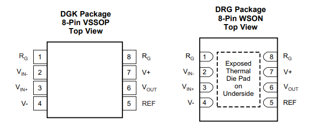
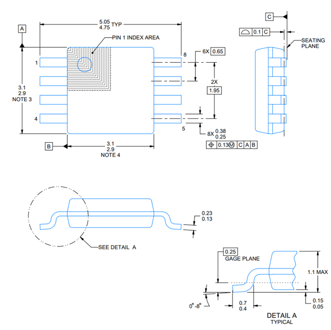
| Package Options | 8-Pin VSSOP, 8-Pin WSON |
| Junction-to-Ambient Thermal Resistance (VSSOP) | 169.5 °C/W |
| Junction-to-Ambient Thermal Resistance (WSON) | 60 °C/W |
| Low-Power Operation | Yes |
| Precision Performance | High Accuracy, Low Drift, Low Noise |
| Pin No. | Pin Name | I/O | Function |
| 1 | RG | — | Gain-setting pin. Connect a gain resistor between Pins 1 and 8 to set the amplifier gain above 1. |
| 2 | VIN− | Input | Inverting (negative) differential input signal. |
| 3 | VIN+ | Input | Non-inverting (positive) differential input signal. |
| 4 | V− | Power | Negative power supply connection. |
| 5 | REF | Input | Reference voltage input that sets the output reference level. Typically connected to ground in single-supply systems. |
| 6 | VOUT | Output | Amplified output signal. |
| 7 | V+ | Power | Positive power supply connection. |
| 8 | RG | — | Gain-setting pin. Connect a gain resistor between Pins 1 and 8 to configure the desired gain. |
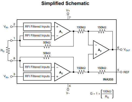
The INA333 uses a three-op-amp instrumentation amplifier architecture to accurately amplify small differential signals while rejecting unwanted noise. As shown in the diagram, the input signals enter through VIN+ and VIN−, where integrated RFI-filtered inputs help reduce radio-frequency interference before amplification.
The first stage consists of amplifiers A1 and A2, which amplify the differential voltage between the two input signals. The gain is determined by the external resistor RG connected between Pins 1 and 8. A smaller RG value produces a higher gain according to the equation G = 1 + (100 kΩ / RG).
The amplified signals are then sent to amplifier A3, which acts as a differential amplifier. This stage subtracts the two amplified signals, rejects common-mode noise, and produces a precise output voltage at VOUT. The REF pin allows the output voltage level to be shifted when required, while V+ and V− provide the power supply for the device.
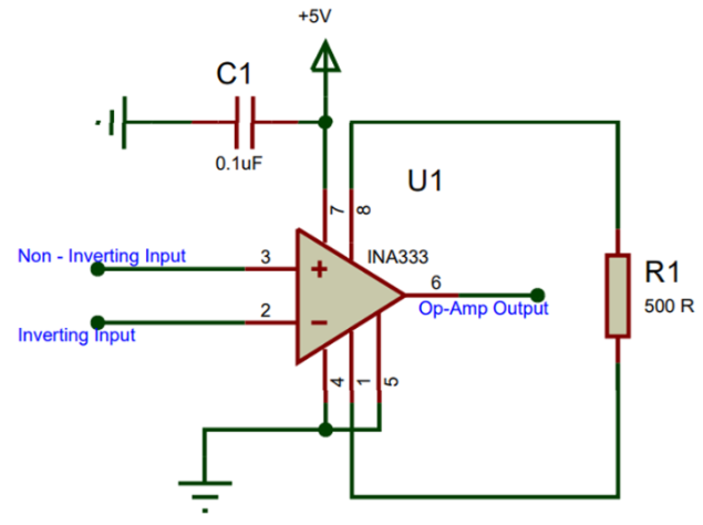
The INA333 can be used as a precision amplifier for small sensor signals. In this circuit, Pin 7 is connected to the +5 V supply, while Pin 4 is connected to ground. A 0.1 μF bypass capacitor is placed near the supply pin to reduce power noise and help keep the circuit stable.
The input signal is connected to VIN+ and VIN−, and the gain is set by resistor R1 between Pins 1 and 8. With a 500 Ω gain resistor, the gain is about 201 using the formula G = 1 + (100 kΩ / RG). The REF pin is connected to ground, so the output is referenced to 0 V. The amplified signal is taken from Pin 6 and can be sent to an ADC, microcontroller, or measurement circuit.
The INA333 is commonly used in electronic weighing scales to amplify the very small voltage signals from load cells. Its low offset voltage and high accuracy help produce stable and precise weight readings, even when measuring small load changes.
Medical devices often measure weak biological signals that need accurate amplification. The INA333 helps improve signal quality by amplifying low-level signals while reducing unwanted electrical noise.
The INA333 is useful in industrial monitoring, data acquisition systems, and environmental sensing equipment. It amplifies small sensor outputs from pressure, force, temperature, and other measurement devices before the signals are processed by an ADC, controller, or recording system.
Because of its low power consumption, the INA333 is suitable for handheld meters, portable test tools, and battery-powered sensor systems. It helps extend battery life while still providing accurate amplification for small signals.
| Specification | INA333 | INA317 | AD623 | AD8226 | INA826 | AD620 |
| Manufacturer | Texas Instruments | Texas Instruments | Analog Devices | Analog Devices | Texas Instruments | Analog Devices |
| Supply Voltage Range | 1.8 V to 5.5 V | 1.8 V to 5.5 V | 3 V to 12 V | 2.2 V to 36 V | 2.7 V to 36 V | ±2.3 V to ±18 V |
| Quiescent Current | 50 μA | 50 μA | 550 μA | 350 μA | 200 μA | 1.3 mA |
| Input Offset Voltage (Max) | 25 μV | 25 μV | 200 μV | 35 μV | 125 μV | 50 μV |
| Offset Drift | 0.1 μV/°C | 0.1 μV/°C | 2 μV/°C | 0.3 μV/°C | 0.4 μV/°C | 0.6 μV/°C |
| Input Bias Current | 200 pA | 200 pA | 25 nA | 300 pA | 5 nA | 1 nA |
| CMRR (Min) | 100 dB | 100 dB | 90 dB | 100 dB | 100 dB | 100 dB |
| Input Noise Density | 50 nV/√Hz | 50 nV/√Hz | 35 nV/√Hz | 22 nV/√Hz | 28 nV/√Hz | 9 nV/√Hz |
| Gain Range | 1 to 1000 | 1 to 1000 | 1 to 1000 | 1 to 1000 | 1 to 10,000 | 1 to 10,000 |
| Gain Set Method | Single Resistor | Single Resistor | Single Resistor | Single Resistor | Single Resistor | Single Resistor |
| Rail-to-Rail Output | Yes | Yes | Near Rail-to-Rail | Yes | No | No |
| Operating Temperature | -40°C to +125°C | -40°C to +125°C | -40°C to +85°C | -40°C to +125°C | -40°C to +125°C | -40°C to +85°C |
| Package Options | VSSOP, WSON | VSSOP, WSON | SOIC, MSOP | MSOP | SOIC, VSSOP | DIP, SOIC |
| Main Strength | Ultra-Low Power | Direct Replacement | Low Cost | Low Noise | Wide Supply Range | High Precision |
Texas Instruments is a leading analog IC manufacturer. It has strong experience in making precision amplifiers like the INA333. The company uses advanced semiconductor processes, automated wafer fabrication, and strict testing systems. These help the INA333 achieve low offset voltage, low drift, low noise, and stable performance. Texas Instruments also uses quality control and reliability testing to support operation across a wide temperature range. Its global manufacturing network helps ensure consistent supply and product quality.

 FPGA / CPLD
 Memory
 MOS
MOS  MCU
MCU  DSP
DSP OCEP
OCEP Secondary
  Other
Other