
075582814553

A high-frequency inverter is an important circuit used to convert DC power into AC power for electronic and power control applications. In this design, the IR2110 driver plays a key role because it allows the control circuit to drive high-side and low-side MOSFETs safely and efficiently. This article explains the design and implementation of an IR2110-based high-frequency inverter in a practical way. It covers the system structure, IR2110 driver operation, PIC16F716 microcontroller control, PWM signal generation, full-bridge MOSFET switching, output filtering, and protection methods.
IR2110 Driver Circuit
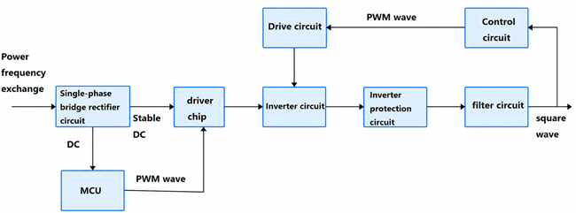
The figure below shows the overall structure of the high-frequency inverter system. The power flow starts from the AC input, which is first sent to a single-phase bridge rectifier. The rectifier converts the AC input into DC voltage, forming the DC bus that supplies the inverter power stage.
After rectification, the DC bus also supplies the regulator circuits. These regulators provide stable 15 V and 5 V outputs for the control and driver sections. The 15 V supply is commonly used by the gate driver stage, while the 5 V supply is used by the microcontroller and other low-voltage control circuits.
The driver stage acts as the link between the control circuit and the power switching stage. It strengthens the control signals and provides the correct gate-drive level needed by the MOSFETs. This allows the inverter stage to switch the DC bus voltage efficiently and convert it into a high-frequency AC waveform.
System Design Scheme
The inverter stage is the main power conversion section of the system. It uses the driven MOSFETs to change the DC supply into an alternating output. Since the switching process creates high-frequency components and electrical noise, the output passes through a filter circuit before reaching the load. The filter helps reduce harmonics and improves the quality of the output waveform.
The system also includes a protection stage to improve safety and reliability. This stage helps detect abnormal conditions such as overcurrent, short circuit, or unstable operation. When a fault is detected, the protection circuit can limit or stop operation to prevent damage to the power devices.
A feedback loop is used to monitor the output condition and support stable operation. By feeding output information back to the control section, the system
The hardware design of the inverter is built around two main control parts: the IR2110 MOSFET driver circuit and the PIC16F716 microcontroller circuit. The microcontroller generates the PWM control signals, while the IR2110 increases these signals to the proper gate-drive level needed to switch the power MOSFETs. Together, these circuits allow the inverter to convert DC power into a controlled AC output.
The IR2110 is a high-side and low-side MOSFET driver commonly used in inverter circuits, motor drives, switching power supplies, and other power conversion systems. It was originally developed by International Rectifier, which is now part of Infineon Technologies. The device is useful because it can drive both the upper and lower MOSFETs in a half-bridge circuit.
In this inverter design, the IR2110 receives low-voltage PWM signals from the microcontroller and converts them into stronger gate-drive signals for the MOSFETs. This is important because a microcontroller pin cannot directly drive power MOSFET gates in a high-voltage inverter stage. The MOSFETs need enough gate voltage and fast switching current to turn on and off efficiently.
The IR2110 includes logic input control, level shifting, high-side output drive, low-side output drive, and undervoltage protection. Its level-shifting function allows the high-side MOSFET gate to be driven even when the MOSFET source terminal rises with the switching node. This makes the device suitable for bridge inverter circuits where the upper MOSFET source is not fixed to ground.
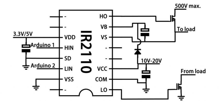
The circuit below includes a bootstrap diode VD1, a bootstrap capacitor C1, a supply filter capacitor C2, and two external MOSFETs labeled S1 and S2. The high-side output HO drives the gate of the upper MOSFET S1, while the low-side output LO drives the gate of the lower MOSFET S2.
The bootstrap circuit is used to create the floating supply needed for the high-side driver. When the lower MOSFET S2 is turned on, the switching node is pulled near ground. During this time, the bootstrap capacitor C1 charges from VCC through the bootstrap diode VD1. Once C1 is charged, it can supply the high-side driver when S1 needs to turn on.
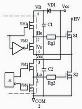
IR2110 Half-Bridge Driver Circuit
When the high-side input signal is active, the IR2110 uses the stored charge in C1 to raise the gate voltage of S1 above its source voltage. This allows the upper MOSFET to turn on properly. When the high-side signal is removed, the gate charge of S1 is discharged through the driver path, turning S1 off.
The low-side MOSFET S2 is controlled by the LO output. When the low-side input is active, LO drives the gate of S2 and turns it on. The high-side and low-side MOSFETs must not turn on at the same time because this would create shoot-through, where current flows directly from the high-voltage DC bus to ground. To prevent this, the control program must insert a short dead time between the switching of S1 and S2.
The inverter circuit use two IR2110 driver ICs. Each IR2110 controls one half-bridge section, so two driver chips are used to control four MOSFETs in a full-bridge inverter. The MOSFETs are arranged as upper and lower switches on each side of the bridge.
The PIC16F716 microcontroller provides the PWM control signals for the driver chips. These signals control the switching sequence of the four MOSFETs. In a full-bridge inverter, diagonal MOSFET pairs are usually switched together to create alternating current flow through the load. For example, one diagonal pair turns on to make current flow in one direction, and the opposite pair turns on to make current flow in the reverse direction.
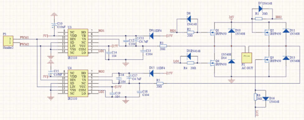
IR2110 Inverter Schematic Diagram
The IR2110 driver chips strengthen the PWM signals and provide the correct gate-drive voltage for the MOSFETs. The bootstrap capacitors and diodes in the circuit help supply the high-side driver sections. Gate resistors are also used to control the MOSFET switching speed and reduce ringing, noise, and switching stress.
As shown in the figure above, the output is taken from the bridge section and delivered to the load. Because the MOSFETs switch rapidly, the control signals must be carefully timed. Dead time is required between the upper and lower switches of the same bridge leg to prevent short circuits. Proper timing, stable gate drive, and correct bootstrap capacitor selection are important for safe inverter operation.
The PIC16F716 microcontroller serves as the main control device in the inverter system. It is suitable for compact inverter designs because it has built-in peripheral functions, low power consumption, and enough I/O pins for basic control and monitoring tasks. In this hardware section, the focus is on the support circuit that allows the microcontroller to operate reliably.
The PIC16F716 circuit uses a regulated 5 V supply. This stable supply voltage is important because the microcontroller must operate within its required voltage range to avoid reset problems, unstable logic levels, or incorrect control output. Proper power supply filtering should also be used near the MCU pins to reduce noise from the inverter power stage.
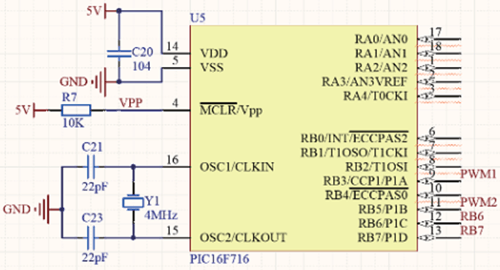
PIC16F716 Peripheral Circuit Diagram
The oscillator circuit provides the clock signal needed for program execution. In this design, a 4 MHz crystal oscillator is connected to the oscillator pins of the PIC16F716. The capacitors connected to the crystal help stabilize oscillation and allow the microcontroller to run at a steady clock frequency.
The reset circuit is connected to the MCLR/VPP pin. A pull-up resistor keeps this pin at the normal operating level during system operation. This allows the microcontroller to start correctly when power is applied and helps prevent unwanted resets caused by noise or unstable supply conditions.
The I/O pins of the PIC16F716 are connected to the IR2110 driver circuit and other control-related parts of the inverter. These pins provide the control interface between the microcontroller and the driver stage. Some pins may also be used for feedback or protection signals, depending on the final circuit design.
The software design is responsible for generating the control signals used by the inverter. In this design, the PIC16F716 uses its Enhanced Capture/Compare/PWM (ECCP) module to produce PWM signals for the IR2110 driver circuit. Proper software configuration is important because it determines the switching frequency, duty cycle, signal timing, and overall inverter performance.
The inverter uses the Enhanced Capture/Compare/PWM module, or ECCP module, of the PIC16F716 microcontroller to generate PWM signals. PWM control is used because it allows the inverter to control the switching state of the MOSFETs by changing the pulse timing and duty cycle.
In this design, the ECCP module is configured to work in half-bridge output mode. This allows the microcontroller to generate two complementary PWM signals. When one output is high, the other output is low. This signal relationship is necessary for controlling the upper and lower MOSFETs of the same inverter bridge leg.
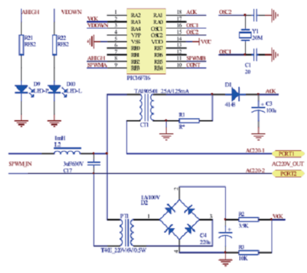
Inverter Protection Circuit
The PWM outputs are sent to the IR2110 driver circuit. The driver then increases the signal strength so the MOSFETs can switch properly. The microcontroller must also add dead time between complementary PWM signals. Dead time is a short delay that prevents the upper and lower MOSFETs from turning on at the same time. Without this delay, shoot-through current may occur and damage the inverter.
The figure above shows the inverter protection circuit connected around the control and power supply sections. The protection circuit helps monitor abnormal output or supply conditions and sends feedback to the microcontroller. This allows the system to reduce switching activity or stop the inverter when a fault is detected.
To generate the PWM waveform, the software must define the PWM period and pulse width. The PWM period determines the output frequency, while the pulse width determines the duty cycle. In the given design example, the target output frequency is 50 Hz and the duty cycle is 30%.
The PWM period is calculated using the basic frequency formula:
T = 1 / f
For a 50 Hz signal:
T = 1 / 50 = 0.02 seconds = 20 ms
If the required duty cycle is 30%, the pulse width is:
Pulse width = 20 ms × 30% = 6 ms
These values are then translated into register settings for the microcontroller. The software sets the ECCP control register, Timer2 register, PWM period register, and pulse width register. Timer2 provides the time base for PWM operation, while the PR2 and CCPR registers define the period and duty cycle.
A simplified configuration process includes setting the ECCP module to PWM mode, enabling dead-time control, configuring Timer2, loading the PWM period value, loading the duty cycle value, and starting the timer. These settings allow the PIC16F716 to continuously generate PWM signals for the IR2110 driver circuit.
In practical inverter software, these values must match the oscillator frequency, timer prescaler, and required switching mode. Correct register calculation is important because wrong timing values can produce unstable output, excessive heat, or incorrect MOSFET switching.
After the software is uploaded to the PIC16F716 microcontroller, the PWM output should be tested with an oscilloscope. Figure 6 shows the measured output waveforms from two microcontroller output pins. The two waveforms are complementary, meaning one signal turns on while the other turns off.

Output Waveform
This complementary waveform confirms that the software is generating the correct switching relationship for the inverter driver stage. The visible separation between switching states also supports safer operation because it helps reduce the risk of both MOSFETs turning on at the same time.
The waveform shown in Figure 6 is not the final filtered AC output. Instead, it represents the control signal used to drive the inverter switches. After these PWM signals pass through the IR2110 driver and the MOSFET bridge, the inverter output can be filtered and shaped into the required AC waveform for the load.
The output stage is responsible for converting DC power into AC power. In this inverter design, four MOSFETs are arranged in a full-bridge configuration and are driven by the IR2110 gate driver circuits. The PIC16F716 microcontroller generates complementary PWM signals that control the switching sequence of the MOSFETs.
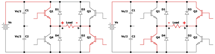
Full-Bridge Inverter Switching Operation
The inverter operates by switching diagonal MOSFET pairs alternately. During one operating state, Q1 and Q2 conduct, allowing current to flow through the load from point a to point b. During the next operating state, Q3 and Q4 conduct, reversing the current flow from point b to point a. This continuous reversal of current creates an alternating voltage across the load.
The PWM signals generated by the microcontroller determine how long each switching pair remains on. By adjusting the PWM duty cycle, the inverter controls the effective output voltage and power delivered to the load. Because the MOSFETs operate primarily in fully switched states, switching losses are minimized and overall conversion efficiency is improved.
Although the load voltage initially consists of high-frequency switching pulses, the alternating current flow shown in the figure above forms the basis of AC waveform generation. After passing through the output filter stage, the waveform becomes smoother and more suitable for practical AC-powered loads.
The output of a PWM inverter contains high-frequency switching components in addition to the desired low-frequency AC waveform. While these switching signals are necessary for inverter operation, they can introduce harmonic distortion, electromagnetic interference (EMI), and additional heating in connected equipment.

PWM Filtering and Sine Wave Reconstruction
To improve waveform quality, the inverter output passes through a filter circuit. The filter commonly consists of inductors and capacitors that attenuate high-frequency switching harmonics while allowing the fundamental AC frequency to pass through. As a result, the output waveform becomes smoother and closer to a sinusoidal waveform.
Better filtering improves the performance of motors, transformers, power supplies, and sensitive electronic equipment. Reduced harmonic content also lowers electrical noise and improves overall system efficiency. The quality of the filter design directly affects output waveform purity and load compatibility.
Without proper filtering, the inverter output may resemble a square wave or heavily distorted PWM waveform. Although some loads can operate under these conditions, many devices achieve better performance and reliability when supplied with a cleaner waveform.
Protection is essential in a high-frequency inverter because power MOSFETs switch large currents at high speed. Without proper protection, electrical faults can damage the inverter within milliseconds.
• Overcurrent Protection - Overcurrent protection detects excessive current caused by overloads or short circuits. When the current becomes too high, the protection circuit can reduce the PWM duty cycle or shut down the inverter completely. This helps protect the MOSFETs, IR2110 driver circuits, and power supply components from permanent damage.
• Dead-Time Control - Dead-time control adds a short delay between complementary PWM switching signals. This delay prevents the upper and lower MOSFETs in the same bridge leg from turning on at the same time. Without dead time, shoot-through current can flow directly through the bridge and quickly destroy the switching devices.
• Undervoltage Protection - Undervoltage protection prevents the IR2110 driver and MOSFETs from operating when the supply voltage is too low. If the gate-drive voltage is insufficient, the MOSFETs may not turn on fully, which increases switching losses and heat. Keeping the driver voltage within a safe range improves efficiency and reliability.
• Thermal Management - Thermal management helps control the heat produced by the MOSFETs and other power components. Heat sinks, good PCB layout, proper spacing, and adequate ventilation help maintain safe operating temperatures. Lower temperatures reduce electrical stress and improve the long-term life of the inverter.
• Short-Circuit Protection - Short-circuit protection responds when the output or load creates an abnormal current path. The system should quickly disable the PWM signal or disconnect the output to prevent severe damage. This protection is especially important in high-frequency inverter circuits because faults can rise very quickly.
• Reliable Software Control - Reliable software control allows the microcontroller to monitor operating conditions and adjust the PWM output when needed. The PIC16F716 can support safer operation by managing dead time, switching sequence, and fault response logic. Good software control helps the inverter remain stable under changing load conditions.
• UPS Systems - Used to convert battery DC power into AC power during power outages.
• Solar Inverters - Convert DC power from solar panels or batteries into usable AC power.
• Portable Power Supplies - Used in compact power stations because high-frequency designs can be smaller and lighter.
• Motor Drives - Control motor speed and output power using PWM switching.
• Industrial Equipment - Provide controlled AC power for machines, automation systems, and power converters.
• Emergency Backup Power - Keep lights, communication devices, and security systems running during power failures.
• Educational Projects - Used for learning inverter design, MOSFET driving, and PWM control.
The IR2110-based high-frequency inverter combines PWM control, MOSFET switching, and gate-driver technology to efficiently convert DC power into AC power. By using the PIC16F716 microcontroller and IR2110 driver, the system can achieve reliable switching performance, stable output operation, and improved power conversion efficiency. With proper filtering and protection features, this inverter design provides a practical solution for power supplies, motor drives, backup systems, and other power electronics applications.

 FPGA / CPLD
 Memory
 MOS
MOS  MCU
MCU  DSP
DSP OCEP
OCEP Secondary
  Other
Other