
075582814553

The JRC4558 dual operational amplifier is designed to amplify and process small electrical signals. It contains two independent op-amps in one package, making it useful for circuits that need more than one signal-processing stage without adding extra ICs. This article explains the JRC4558’s key features, specifications, pin functions, working principle, circuit behavior, package dimensions, and comparison with other popular op-amps.
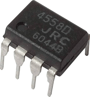
The <a href="https://www.y-ic.com/pdf/JRC/JRC4558.html" target="_blank" "="" style="cursor: pointer; color: rgb(0, 0, 238); font-weight: bold;">JRC4558 Dual Operational Amplifier is an integrated circuit that contains two independent operational amplifiers in one package. It is designed to amplify small analog signals and support stable signal processing in electronic circuits.
Each amplifier inside the JRC4558 has high voltage gain and can be configured with external components to control gain, feedback, and signal response. Its dual-channel structure helps reduce component count and saves PCB space compared with using two separate op-amp ICs.
The JRC4558 is valued for its simple design, stable operation, wide availability, and cost-effective performance. While newer op-amps may offer lower noise or faster response, the JRC4558 remains a practical choice for many general analog circuit designs.
If you are interested in purchasing the JRC4558 dual operational amplifier, feel free to contact us for pricing and availability.
| Parameter | Specification |
| Device Type | Dual Operational Amplifier |
| Number of Amplifiers | 2 |
| Frequency Compensation | Internally compensated |
| Latch-Up Protection | No latch-up |
| Common-Mode Voltage Range | Large common-mode input range |
| Differential Input Voltage Range | Wide differential input range |
| Channel Matching | Gain and phase matched amplifiers |
| Input Transistor Type | Low-noise input transistors |
| Pin Compatibility | MC1458, LM358 compatible |
| Supply Voltage (Max) | ±22 V |
| Differential Input Voltage (Max) | ±18 V |
| Input Voltage (Max) | ±15 V |
| Operating Temperature Range | -20°C to +85°C |
| Storage Temperature Range | -65°C to +150°C |
| Power Dissipation (PDIP-8) | 600 mW |
| Power Dissipation (SOP-8) | 400 mW |
| Supply Current | 2.3 mA to 4.5 mA |
| Input Offset Voltage | 2 – 6 mV |
| Input Offset Current | 5 nA - 200 nA |
| Input Bias Current | 30 – 500 nA |
| Large Signal Voltage Gain (Min) | 20 V/mV - 200 V/mV |
| Common-Mode Input Voltage Range (Min) | ±12 V - ±13 V |
| Common-Mode Rejection Ratio | 70 – 90 dB |
| Power Supply Rejection Ratio | 76 – 90 dB |
| Output Voltage Swing (Typ) | ±12 V |
| Output Voltage Swing (Max) | ±14 V |
| Power Consumption (Typ) | 70 mW |
| Power Consumption (Max) | 170 mW |
| Slew Rate | 1.2 - 2.2 V/μs |
| Rise Time (Typ) | 0.3 μs |
| Overshoot (Typ) | 15% |
| Input Resistance (Min) | 0.3 - 2MΩ |
| Output Resistance (Typ) | 75 Ω |
| Total Harmonic Distortion (Typ) | 0.008% |
| Channel Separation (Typ) | 120 dB |
| Unity Gain Bandwidth | 2.0 to 2.8 MHz |
| Package Options | PDIP-8, SOP-8 |
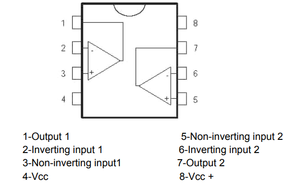
| Pin No. | Pin Name | Function Description |
| 1 | Output 1 | Output terminal of the first operational amplifier. The amplified signal from Op-Amp 1 appears at this pin. |
| 2 | Inverting Input 1 (-) | Inverting input of the first amplifier. A signal applied here produces an output that is 180° out of phase with the input. |
| 3 | Non-Inverting Input 1 (+) | Non-inverting input of the first amplifier. A signal applied here produces an output that is in phase with the input. |
| 4 | VCC− | Negative power supply terminal. In dual-supply circuits, this pin is connected to the negative voltage rail. |
| 5 | Non-Inverting Input 2 (+) | Non-inverting input of the second amplifier. Signals applied to this pin are amplified without phase inversion. |
| 6 | Inverting Input 2 (-) | Inverting input of the second amplifier. Signals applied here are amplified with phase inversion. |
| 7 | Output 2 | Output terminal of the second operational amplifier. The amplified signal from Op-Amp 2 appears at this pin. |
| 8 | VCC+ | Positive power supply terminal. This pin supplies operating voltage to both amplifiers inside the IC. |
The JRC4558 amplifies analog signals through several internal transistor stages that work together to provide voltage gain, signal conditioning, and output drive capability. As shown in the internal circuit diagram, the amplification process begins at the differential input stage, where transistors compare the voltage difference between the non-inverting (+IN) and inverting (-IN) inputs. Rather than amplifying each input independently, the device amplifies the difference between the two signals. This differential operation helps reject common-mode noise and improves overall signal accuracy.
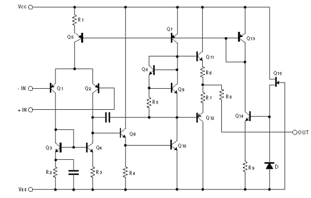
After the input signal is detected, it passes through intermediate transistor stages that provide most of the voltage amplification. These stages increase the signal amplitude while maintaining linear operation. The JRC4558 also includes internal frequency compensation, which helps stabilize the amplifier and reduces the risk of unwanted oscillation. This compensation allows the device to operate reliably in a wide range of circuit configurations without requiring external compensation components.
The amplified signal is then delivered to the output stage, where additional transistors provide the current needed to drive external loads. In most circuits, a portion of the output signal is fed back to the inverting input through a feedback network. This negative feedback controls the amplifier gain, improves stability, reduces distortion, and helps achieve the desired circuit performance. Through this multi-stage architecture, the JRC4558 can accurately process and amplify low-level analog signals while maintaining stable operation and good signal quality.
The circuit diagram shows a practical audio signal processing circuit built around the dual amplifiers inside the JRC4558. Both operational amplifiers are used together to process the input signal before delivering the final output. The first amplifier stage receives the input signal through resistor R1 and uses a feedback network to control gain and signal behavior. Diodes D1 and D2 are connected in the feedback path and act as clipping elements. When the signal amplitude exceeds the forward voltage of the diodes, they begin conducting and limit the signal peaks. This creates a controlled clipping effect that modifies the waveform and introduces harmonic distortion.
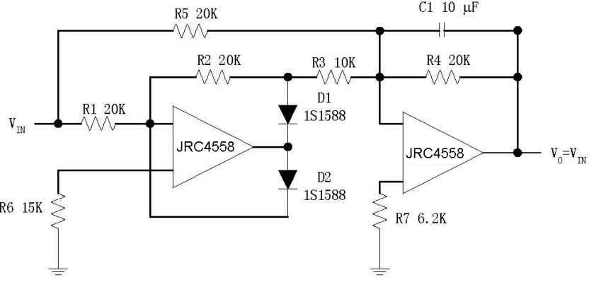
The clipped signal is then passed to the second JRC4558 amplifier stage through a network of resistors and capacitor C1. This stage provides additional amplification, filtering, and signal shaping. The resistor network determines the gain and frequency response, while capacitor C1 helps control the circuit's tonal characteristics by affecting how different frequencies are processed. The second amplifier also buffers the signal, helping maintain a stable output level.
In real-world applications, this type of circuit is commonly used for analog signal conditioning and audio processing. The first op-amp stage performs amplification and clipping, while the second stage refines the processed signal and drives the output. This demonstrates how the JRC4558 can be used not only as a simple amplifier but also as an active signal-processing device capable of combining amplification, feedback control, filtering, and waveform modification within a single circuit design.
The diagram also illustrates one of the key advantages of the JRC4558's dual-op-amp architecture. Since two independent amplifiers are available in the same package, designers can create multiple signal-processing stages without requiring additional ICs. This reduces component count, saves board space, simplifies circuit design, and lowers overall system cost while maintaining reliable analog performance.
| Parameter | JRC4558 | LM358 | NE5532 | TL072 |
| Number of Amplifiers | 2 | 2 | 2 | 2 |
| Supply Voltage Range | ±5V to ±15V | 3V to 32V / ±1.5V to ±16V | ±3V to ±20V | ±5V to ±18V |
| Unity Gain Bandwidth | 2.8 MHz | 1 MHz | 10 MHz | 3 MHz |
| Slew Rate | 2.2 V/μs | 0.3 V/μs | 9 V/μs | 13 V/μs |
| Input Offset Voltage (Typ) | 2 mV | 2 mV | 0.5 mV | 3 mV |
| Input Bias Current (Typ) | 30 nA | 20 nA | 200 nA | 65 pA |
| Input Resistance (Typ) | 2 MΩ | 10 MΩ | 300 kΩ | 10¹² Ω |
| Supply Current (Typ) | 2.3 mA | 0.7 mA | 8 mA | 2.8 mA |
| Output Voltage Swing (Typ) | ±12 V | VCC − 1.5 V | ±13 V | ±13.5 V |
| THD (Typ) | 0.008% | 0.02% | 0.0005% | 0.003% |
| Noise Density (Typ) | ~8 nV/√Hz | ~40 nV/√Hz | ~5 nV/√Hz | ~18 nV/√Hz |
| Common-Mode Rejection Ratio (Typ) | 90 dB | 85 dB | 100 dB | 100 dB |
| Power Supply Rejection Ratio (Typ) | 90 dB | 100 dB | 100 dB | 100 dB |
| Operating Temperature Range | -20°C to +85°C | 0°C to +70°C | 0°C to +70°C | -40°C to +85°C |
The JRC4558 continues to provide reliable signal amplification for a wide range of analog circuit designs. Understanding its specifications, pin functions, internal operation, and real-world circuit behavior allows you to use the device more effectively and avoid common design limitations. The dual-op-amp architecture also enables multiple signal-processing stages within a single package, helping reduce component count and simplify circuit layouts.

 FPGA / CPLD
 Memory
 MOS
MOS  MCU
MCU  DSP
DSP OCEP
OCEP Secondary
  Other
Other