
075582814553

The CD4026B is a useful CMOS counter IC for circuits that need to count pulses and show numbers on a 7-segment display. Instead of using a separate counter IC and a separate display decoder, the CD4026B combines both functions in one device. This article explains the CD4026B pinout, internal operation, electrical specifications, display connection, two-digit counter circuit, and more.
The CD4026B is a CMOS decade counter with a built-in 7-segment display decoder. It counts clock pulses from 0 to 9 and converts the internal Johnson counter output into signals that can drive one numeric display digit.
The IC includes common control pins such as CLOCK, RESET, and CLOCK INHIBIT. A high RESET signal clears the counter to zero, while the CLOCK INHIBIT pin can stop counting without clearing the current value. The CD4026B also provides CARRY OUT, seven decoded segment outputs a–g, DISPLAY ENABLE, and an ungated C-segment output. Its low power use and reduced external component count make it practical for simple numeric display circuits.
If you are interested in purchasing the CD4026B, feel free to contact us for pricing and availability.
| Orderable Device | Status | Package Type | Package Drawing | Pins | Package Qty | Eco Plan | Lead/Ball Finish | MSL Peak Temp | Op Temp (°C) |
| CD4026BEE4 | ACTIVE | PDIP | N | 16 | 25 | Pb-Free (RoHS) | CU NIPDAU | N/A for Pkg Type | -55 to 125 |
| CD4026BPW | ACTIVE | TSSOP | PW | 16 | 90 | Green (RoHS & no Sb/Br) | CU NIPDAU | Level-1-260C-UNLIM | -55 to 125 |
| CD4026BPWR | ACTIVE | TSSOP | PW | 16 | 2000 | Green (RoHS & no Sb/Br) | CU NIPDAU | Level-1-260C-UNLIM | -55 to 125 |
| CD4033BPW | ACTIVE | TSSOP | PW | 16 | 90 | Green (RoHS & no Sb/Br) | CU NIPDAU | Level-1-260C-UNLIM | -55 to 125 |
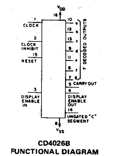
| Pin Number | Pin Name | Function |
| 1 | CLOCK (CLK) | Receives clock pulses that advance the counter from 0 to 9. The count increases on each positive clock transition. |
| 2 | CLOCK INHIBIT | Enables or disables counting. A LOW signal allows clock pulses to reach the counter, while a HIGH signal stops counting. |
| 3 | DISPLAY ENABLE IN | Controls display output operation. Used to enable or blank the 7-segment display outputs. |
| 4 | DISPLAY ENABLE OUT | Provides a display enable signal for cascading multiple CD4026B ICs in multi-digit display systems. |
| 5 | CARRY OUT | Generates an output pulse after the counter completes one full decade (0–9). Used for cascading additional counters. |
| 6 | f SEGMENT OUTPUT | Drives segment f of a common-cathode 7-segment display. |
| 7 | g SEGMENT OUTPUT | Drives segment g of a common-cathode 7-segment display. |
| 8 | VSS | Ground connection (0 V reference) for the IC. |
| 9 | d SEGMENT OUTPUT | Drives segment d of a common-cathode 7-segment display. |
| 10 | a SEGMENT OUTPUT | Drives segment a of a common-cathode 7-segment display. |
| 11 | e SEGMENT OUTPUT | Drives segment e of a common-cathode 7-segment display. |
| 12 | b SEGMENT OUTPUT | Drives segment b of a common-cathode 7-segment display. |
| 13 | c SEGMENT OUTPUT | Drives segment c of a common-cathode 7-segment display. |
| 14 | UNGATED "c" SEGMENT OUT | Provides a direct segment c output that is not affected by display enable control logic. |
| 15 | RESET | Resets the counter to zero and updates the display to show digit 0. |
| 16 | VDD | Positive power supply input for the IC. Typical operating voltage ranges from 3 V to 15 V. |
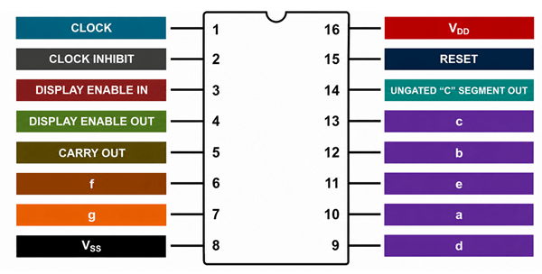
As shown in the functional diagram, the CD4026B combines a decade counter and a 7-segment display driver into a single integrated circuit. The CLOCK input receives pulses that advance the count from 0 to 9, while the RESET input returns the counter to zero whenever a logic HIGH signal is applied. The CLOCK INHIBIT input can temporarily stop counting without clearing the displayed number. After processing each clock pulse, the internal counter sends the count value to the decoder section, which activates the appropriate segment outputs (a–g) to display the corresponding digit on a common-cathode 7-segment display. The diagram also shows the CARRY OUT output, which generates a pulse after every ten counts and is used for cascading additional CD4026B devices in multi-digit display systems. Other control signals, including DISPLAY ENABLE IN, DISPLAY ENABLE OUT, and the UNGATED "C" SEGMENT output, provide additional display control functions.
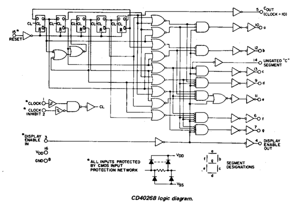
The logic diagram provides a detailed view of the internal circuitry that allows the CD4026B to perform counting and display decoding. As shown in the diagram, the device contains a five-stage Johnson counter formed by interconnected flip-flops that generate a sequence of ten unique count states. These count states are processed by a network of logic gates that decode the counter outputs into the correct segment control signals for the 7-segment display. The diagram also illustrates how the CLOCK, CLOCK INHIBIT, and RESET signals interact with the counter stages to control counting operation. The logic circuitry generates the seven decoded outputs (a–g) as well as the CARRY OUT signal used for cascading counters. This internal architecture eliminates the need for a separate BCD decoder, allowing the CD4026B to directly drive a display while maintaining a relatively simple external circuit.
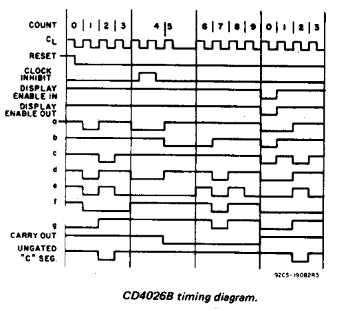
The timing diagram illustrates how the CD4026B responds to clock pulses and how its outputs change over time. As shown in the diagram, the counter advances one count on each positive transition of the CLOCK signal, causing the displayed value to progress from 0 through 9 before returning to 0. The waveform also demonstrates the effect of the RESET input, which immediately clears the counter and forces the display back to zero. When the CLOCK INHIBIT signal becomes active, incoming clock pulses are ignored and the displayed value remains unchanged. The timing diagram further shows the operation of DISPLAY ENABLE IN and DISPLAY ENABLE OUT, which control whether the decoded segment outputs are visible on the display. The segment output waveforms (a–g) change according to the current count value, producing the correct digit patterns on the 7-segment display. In addition, the CARRY OUT waveform generates one pulse for every complete counting cycle, allowing multiple CD4026B devices to be synchronized in multi-digit counter applications.
| Parameter | Specification |
| Supply Voltage (VDD) | 3 V to 15 V |
| Recommended Operating Voltage | 5 V to 10 V |
| Supply Current | Typically less than 1 µA (static) |
| Clock Input Type | Positive-edge triggered |
| Maximum Clock Frequency | Up to approximately 6 MHz at 10 V |
| Count Range | 0 to 9 |
| Output Type | Decoded 7-segment outputs (a–g) |
| Output Drive Capability | Suitable for CMOS loads and LED segment driving |
| Carry-Out Output Frequency | Clock frequency ÷ 10 |
| Reset Response | Asynchronous reset |
| Operating Temperature Range | -55°C to +125°C |
| Package Options | PDIP, SOIC, TSSOP |
The CD4026B is designed to directly drive a common-cathode 7-segment display, eliminating the need for a separate BCD-to-7-segment decoder. As shown in the circuit diagram, the segment outputs (A–G) of the CD4026B are connected directly to the corresponding display segments. When clock pulses are applied to the CLK input, the IC automatically counts from 0 to 9 and activates the correct segment combinations to display each digit.
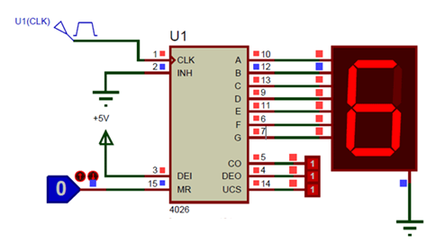
In this example, the Clock Inhibit (INH) pin is connected to ground, allowing the counter to respond to incoming clock pulses. The Display Enable In (DEI) pin is connected to the positive supply voltage to keep the display active, while the Master Reset (MR) pin remains low during normal operation. The common cathode terminal of the display is connected to ground, enabling the CD4026B outputs to illuminate the required segments.
The CD4026B outputs are labeled A, B, C, D, E, F, and G, corresponding directly to the seven segments of the display. As the counter advances, the IC internally decodes the count value and drives the appropriate segments without requiring additional logic circuitry. This simplifies circuit design and makes the CD4026B a popular choice for digital counters, timers, event counters, and display projects.
The circuit diagram shows a practical two-digit counter built using two CD4026B decade counter and 7-segment display driver ICs. The system is powered from a 6 V supply and uses two common-cathode 7-segment displays to show count values from 00 to 99. Each CD4026B combines a decade counter and a 7-segment decoder, allowing it to directly drive a display without requiring additional decoding circuitry. This simplifies the design and reduces the number of external components needed for multi-digit counting applications.
The lower CD4026B (IC1) functions as the units counter. Clock pulses generated by the sensor input circuit are applied to its CLK pin, causing the displayed value to increase by one for each detected event. Internally, the IC counts from 0 to 9 and automatically activates the appropriate segment outputs (a–g) to display the corresponding digit on the first 7-segment display. When the count reaches 9 and another pulse arrives, the counter returns to 0 and generates a carry-out pulse.
The carry-out output of IC1 is connected to the clock input of the upper CD4026B (IC2), creating a cascaded counter arrangement. Each time IC1 completes a full counting cycle from 0 to 9, the carry-out pulse increments IC2 by one count. IC2 drives the second 7-segment display, which represents the tens digit. Through this cascading method, the circuit can display numbers from 00 to 99 using only two CD4026B devices.
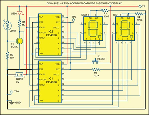
The input sensing section consists of an LDR (light-dependent resistor), a BC547 transistor, and associated resistors. Under normal conditions, the LDR receives light and maintains a specific resistance level. When an object interrupts the light path, the resistance of the LDR changes, causing the transistor to switch states and generate a clock pulse. This pulse is then applied to the counter, increasing the displayed count by one. Because of this arrangement, the circuit can be used as an object counter, people counter, production line counter, or event counter.
The RESET pushbutton (S1) is connected to the reset inputs of both CD4026B ICs. When pressed, it forces both counters back to zero simultaneously, causing the displays to show 00. This feature allows the user to clear the count and begin a new counting cycle without disconnecting power from the circuit.
The resistor network connected to the displays helps limit current and ensures proper segment operation. The common-cathode terminals of the displays are connected according to the requirements of the CD4026B, allowing the IC outputs to directly illuminate the necessary segments. Proper power supply connections to the VDD and VSS pins ensure stable operation of both counters and reliable display performance.
This circuit demonstrates one of the most common uses of the CD4026B: building a multi-digit event counter without a microcontroller. By combining the counter, decoder, and display driver functions into a single IC, the CD4026B provides a simple and cost-effective solution for counting applications that require a numeric visual display.
The CD4026B is commonly used in circuits that count events, objects, or user actions. Each clock pulse increases the displayed number by one, making it useful for button counters, product counters, visitor counters, and sensor-based object detection systems. Sensors such as LDRs, infrared sensors, photodiodes, and proximity sensors can generate the pulses needed by the CD4026B.
In industrial settings, the CD4026B can help monitor repeated machine actions, conveyor items, packaging cycles, motor rotations, and production output. Its carry-out function also allows multiple ICs to be cascaded, so the system can display larger values beyond a single digit.
The CD4026B can be used in simple scoreboard circuits for games, sports, quizzes, and competitions. Push buttons or electronic switches can send clock pulses to the IC, allowing the score to increase each time an input is triggered. For higher scores, several CD4026B ICs can be connected together to create multi-digit displays.
The CD4026B can work with timing circuits, oscillators, or pulse generators to display counted pulses within a time period. This makes it useful in basic frequency counters, elapsed-time displays, and timer circuits where a numerical display is needed without using a microcontroller.
The CD4026B is useful for learning digital electronics because it shows how clock pulses, counters, reset control, cascading, and 7-segment displays work together. Since it already includes the counter and display decoder, students can build practical circuits with fewer parts while still understanding important digital logic concepts.
The CD4026B can be used in simple test instruments that need to display pulse counts during measurement or testing. Its low component count, direct display-driving ability, and easy cascading support make it suitable for compact counters, test benches, and basic electronic measurement setups.
| Problem | Possible Causes | Troubleshooting Steps |
| Display Not Counting | No clock signal, Clock Inhibit pin held HIGH, missing power supply, incorrect wiring | Verify VDD and VSS connections, check that clock pulses reach Pin 1, ensure Clock Inhibit (Pin 2) is LOW, and inspect all wiring connections. |
| Missing Display Segments | Loose connections, damaged display segment, incorrect segment wiring, faulty IC output | Check segment wiring between the CD4026B and display, inspect solder joints, test the display separately, and verify continuity of segment connections. |
| Incorrect Digit Sequence | Noise on clock line, switch bounce, improper cascading connections, unstable power supply | Use a debounced clock source, add filtering if necessary, verify Carry Out connections, and ensure a stable power supply voltage. |
| Counter Skips Numbers | Multiple clock pulses generated unintentionally, noisy input signal, mechanical switch bounce | Add a debouncing circuit, use Schmitt trigger conditioning, shorten noisy signal paths, and verify clock waveform quality with an oscilloscope. |
| Counter Counts Randomly | Floating clock input, electrical interference, poor grounding | Keep unused inputs properly biased, improve grounding, add bypass capacitors, and shield long signal wires from noise sources. |
| Display Always Shows Zero | Reset pin continuously HIGH, no clock pulses present, faulty counter stage | Check that Reset (Pin 15) remains LOW during normal operation, verify clock activity, and inspect reset circuitry for faults. |
| Display Frozen at One Number | Clock Inhibit activated, missing clock signal, damaged clock source | Confirm Clock Inhibit is LOW, verify clock pulse generation, and inspect the pulse source circuitry. |
| Reset Function Not Working | Incorrect reset wiring, faulty pushbutton, insufficient reset voltage | Verify Reset pin connections, test the switch operation, and ensure the reset signal reaches the required logic HIGH level. |
| Multi-Digit Counter Not Advancing | Carry Out not connected properly, faulty cascading wiring, second counter not powered | Check the Carry Out connection from the first CD4026B to the next stage, verify power connections, and inspect clock routing between counters. |
| Dim or Uneven Display Brightness | Insufficient supply voltage, incorrect resistor values, overloaded outputs | Verify supply voltage, check current-limiting resistor values, and ensure display current requirements do not exceed output capabilities. |
| Some Digits Display Incorrectly | Segment wiring errors, faulty display, damaged output pin | Compare wiring against the pinout diagram, test individual display segments, and verify the corresponding CD4026B outputs. |
| Counter Resets Unexpectedly | Power supply noise, unstable reset line, loose connections | Add decoupling capacitors (0.1 µF near VDD), improve reset signal stability, and inspect wiring for intermittent connections. |
| Feature | CD4026B | 74LS90 + 7-Segment Decoder (e.g., 74LS47/74LS48) |
| Counter Function | Integrated decade counter | Decade counter only |
| Display Decoder | Built-in 7-segment decoder | Requires separate decoder IC |
| Number of ICs Required | One IC | Two or more ICs |
| Circuit Complexity | Low | Higher |
| Wiring Effort | Minimal | More extensive |
| PCB Space Required | Smaller | Larger |
| Component Count | Lower | Higher |
| Design Cost | Lower for simple displays | Higher due to additional components |
| Display Type Support | Common-cathode displays | Depends on decoder used |
| Count Range | 0–9 per IC | 0–9 per IC |
| Cascading Capability | Yes, using Carry Out | Yes, using counter outputs |
| Clock Input | Direct clock input | Direct clock input |
| Reset Function | Built-in reset | Built-in reset |
| Leading-Zero Suppression | No | Possible with additional circuitry |
| Display Flexibility | Limited to integrated decoder functions | Greater flexibility with different decoders |
| Troubleshooting Difficulty | Easier | More complex |
| Educational Value | Good for beginners | Better for learning digital logic design |
| Power Consumption | Lower (CMOS) | Higher (TTL) |
| Operating Voltage | 3 V to 15 V | Typically 5 V |
| Noise Immunity | Higher CMOS noise margin | Lower than CMOS devices |
| Best For | Simple counters and display projects | Advanced digital logic systems |
Texas Instruments manufactures the CD4026B using mature CMOS logic production processes designed for low power consumption, stable switching performance, and long-term reliability. Its manufacturing capabilities include semiconductor wafer fabrication, IC assembly, package testing, electrical verification, and quality control. TI supplies the CD4026B in several package types, including PDIP, SOIC, and TSSOP, making it suitable for both through-hole and surface-mount circuit designs. The device is produced to support a wide operating voltage range, industrial temperature performance, RoHS-compliant options, and consistent logic operation. Through its global semiconductor manufacturing and supply chain network, Texas Instruments can support high-volume production, long product availability, and reliable sourcing for customers.

 FPGA / CPLD
 Memory
 MOS
MOS  MCU
MCU  DSP
DSP OCEP
OCEP Secondary
  Other
Other