
075582814553

The CH9102 is a USB to high-speed serial port chip that allows modern computers to communicate with devices that use serial interfaces such as UART, RS232, RS485, and RS422. The CH9102 is designed to provide fast data transfer, stable connections, and flexible voltage compatibility. This article will discuss the CH9102 pinout, working principle, performance, features, applications, comparisons, and design tips to help you decide if it is the right choice for your project.
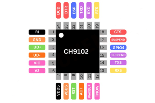
| QFN24 Pin | QFN28 Pin | Pin Name | Type | Description |
| 7 | 7 | VDD5 | Power | Main power supply input (5V). Requires external decoupling capacitor. |
| 5 | V3 → VIO | VIO | Power | I/O voltage supply input. Requires external decoupling capacitor. |
| 2, 0 | 3, 0 | GND | Power | Ground connection. Connect directly to USB ground. |
| 6 | 6, 22 | V3 | Power | Internal regulator output. Connect to VDD5 if <3.6V, otherwise use 0.1µF capacitor. |
| 9 | 9 | RST | Input | External reset input, active low, built-in pull-up resistor. |
| 3 | 4 | UD+ | USB Signal | USB D+ line. Connect directly (no series resistor). |
| 4 | 5 | UD- | USB Signal | USB D− line. Connect directly (no series resistor). |
| 8 | 8 | VBUS | Input | USB VBUS detection input, built-in pull-down resistor. |
| 21 | 26 | TXD | Output | UART transmit data output (idle high). |
| 20 | 25 | RXD | Input | UART receive data input with integrated pull-up. |
| 18 | 23 | CTS | Input | Clear-to-send signal (active low). |
| 22 | 27 | DSR | Input | Data set ready signal (active low). |
| 1 | 2 | RI | Input | Ring indicator signal (active low). |
| 24 | 1 | DCD | Input | Data carrier detect (active low). |
| 23 | 28 | DTR | Output | Data terminal ready (active low). |
| 19 | 24 | RTS | Output | Request to send (active low). |
| 15 | 11 | SUSPEND# | Output | USB suspend state (active low). |
| 17 | 12 | SUSPEND | Output | USB suspend state (active high). |
| 11 | 16 | WAKEUP/GPIO3 | I/O | USB wake-up input (active low) or GPIO3. |
| 12 | 17 | TNOW/GPIO2 | I/O | Transmission status output or GPIO2. |
| 13 | 18 | RXS/GPIO1 | I/O | RX status output or GPIO1. |
| 14 | 19 | TXS/GPIO0 | I/O | TX status output or GPIO0. |
| — | 20 | GPIO6 | I/O | General-purpose I/O (software-controlled). |
| — | 21 | GPIO5 | I/O | General-purpose I/O (software-controlled). |
| 16 | — | GPIO4 | I/O | General-purpose I/O (software-controlled). |
| 10 | 10 | ACT# | Output | USB configuration complete indicator (active low). |
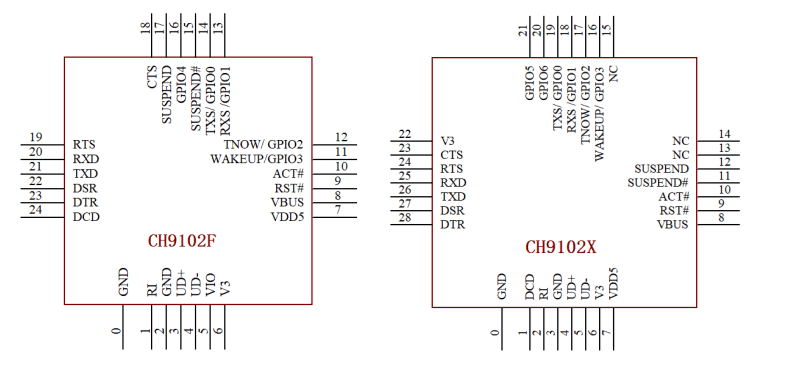
| Package | Body Size | Lead Pitch | Description | Part No. |
| QF24_4X4 | 4 × 4 mm | 0.5 mm (19.7 mil) | Square leadless 24-pin package | CH9102F |
| QF28_5X5 | 5 × 5 mm | 0.5 mm (19.7 mil) | Square leadless 28-pin package | CH9102X |
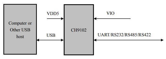
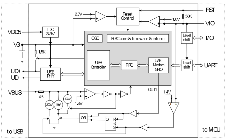
The CH9102 functional block diagram illustrates how the chip connects a USB host, such as a computer, to serial communication interfaces. Data flows from the USB side into the CH9102, where it is converted into serial signals, enabling communication with devices that use UART or related standards.
The diagram also defines the chip’s power structure. The VDD5 pin supplies the main 5V input, while VIO sets the logic level for the I/O pins, allowing compatibility with both 3.3V and 5V systems. This separation improves stability and makes the chip easier to integrate into different hardware designs.
On the output side, the CH9102 supports multiple interfaces, including UART, RS232, RS485, and RS422. This flexibility allows it to be used not only with microcontrollers but also in industrial and long-distance communication systems. Overall, the diagram provides a clear view of how the chip bridges USB and serial communication in practical applications.
The CH9102 operates as a USB-to-serial converter that appears as a virtual COM port when connected to a computer. This allows software to communicate with external devices using standard serial communication, even though the physical interface is USB.
Internally, the chip uses a USB interface engine to manage tasks such as device recognition and data transfer. Incoming USB data is processed by internal control logic and buffers, then converted into UART format with correct timing and baud rate settings. This ensures reliable communication with connected devices.
The converted data is sent through the TXD and RXD pins, enabling direct connection to microcontrollers such as STM32, Arduino, or ESP modules. For more stable high-speed communication, hardware flow control signals like RTS and CTS are also available. When required, external transceivers can extend the interface to RS232 or RS485 standards.
In practical use, the CH9102 enables smooth data exchange between modern USB systems and embedded or industrial devices, making it useful for tasks such as programming, debugging, and real-time data communication.
The CH9102 supports high baud rates (up to several Mbps depending on system configuration), making it suitable for fast data transfer tasks such as firmware flashing and continuous data streaming. In real-world use, it maintains stable communication at common rates like 115200, 921600, and even higher, which is important for modern microcontrollers and high-speed debugging.
Latency is a key factor in applications like debugging and command-response systems. The CH9102 uses internal buffering and efficient USB handling to reduce delay between USB and serial conversion. This results in responsive communication, which is critical when interacting with embedded systems or sending rapid commands during development.
The chip provides consistent performance across Windows, Linux, and macOS, as long as proper drivers are installed. In practical scenarios, users experience stable COM port detection and minimal connection drops, especially when using quality USB cables and correct driver versions.
For applications like data logging and monitoring, the CH9102 can handle continuous data streams without significant packet loss. Its internal control logic ensures proper data framing and synchronization, which helps maintain data integrity over long periods of operation.
When used with external transceivers (e.g., RS485), the CH9102 performs reliably in noisy or long-distance communication environments. This makes it suitable for industrial systems where stable communication is required despite electrical interference.
The separation of VDD5 and VIO power domains allows the chip to adapt to different system voltages while maintaining stable signal levels. This improves overall reliability, especially in mixed-voltage designs and compact embedded systems.
| Category | Parameter | Specification | Description |
| USB Interface | USB Standard | USB 2.0 Full Speed | Compatible with standard USB ports on PCs and embedded hosts |
| Data Transfer Rate | Up to 12 Mbps | Maximum USB full-speed bandwidth | |
| USB Function | USB-to-Serial Bridge | Converts USB data to UART/serial communication | |
| Serial Interface | UART Support | Yes (TXD, RXD) | Standard asynchronous serial communication |
| Additional Interfaces | RS232, RS485, RS422 (via external transceiver) | Extends use to industrial communication systems | |
| Flow Control | RTS, CTS, DTR, DSR, DCD, RI | Supports hardware flow control for stable high-speed data transfer | |
| Baud Rate | Supported Range | Up to several Mbps (commonly up to ~3 Mbps) | Suitable for high-speed data transmission and firmware flashing |
| Voltage & Power | Supply Voltage (VDD5) | 5V | Main power input, typically from USB |
| I/O Voltage (VIO) | 3.3V / 5V (configurable) | Allows compatibility with different logic levels | |
| Internal Regulator (V3) | ~3.3V Output | Used for internal circuits and stability | |
| Signal Pins | TXD / RXD | Serial Data Lines | Used for communication with microcontrollers |
| USB Lines | UD+ / UD− | Direct USB data connection (no series resistor required) | |
| GPIO & Control | GPIO Pins | Multiple (GPIO0–GPIO6 depending on package) | Configurable for custom control or status signals |
| Status Signals | TXS, RXS, TNOW | Indicate transmission and reception status | |
| Suspend Signals | SUSPEND, SUSPEND# | Indicate USB suspend state | |
| Driver Support | Operating Systems | Windows, Linux, macOS | Requires driver installation (auto-supported in many Linux systems) |
| Virtual COM Port | Yes | Appears as standard serial port for software compatibility | |
| Performance | Latency | Low | Suitable for real-time debugging and communication |
| Stability | High | Reliable for continuous data transfer and logging | |
| Packaging | Package Types | QFN24, QFN28 | Compact surface-mount packages for PCB design |
| Applications | Typical Uses | MCU communication, debugging, IoT, industrial systems | Used in Arduino, STM32, ESP-based designs |
The CH9102 application circuit diagram shows how the chip is connected in a real hardware design to enable USB-to-serial communication. At the center is the CH9102 IC, which connects to a USB interface on one side and exposes serial communication pins such as TXD, RXD, RTS, and CTS on the other side. This allows a computer to communicate with external devices like microcontrollers through a standard USB connection.
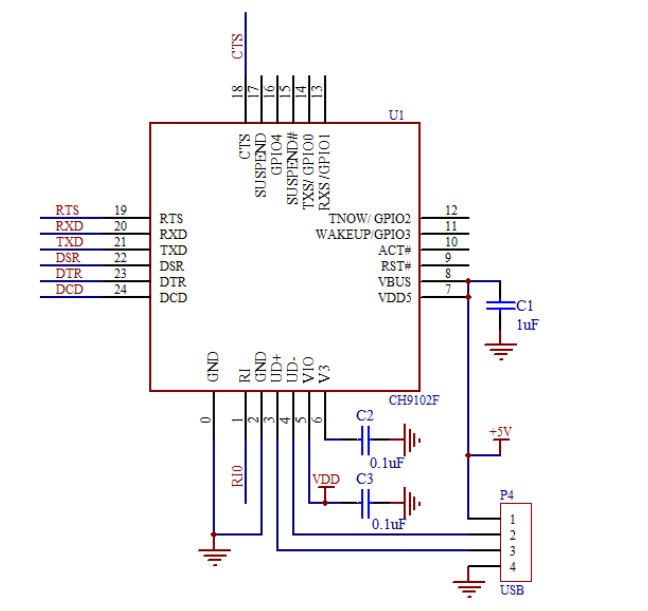
The power section highlights how the chip is supplied and stabilized. The VDD5 pin is connected to the +5V USB power, while capacitors (such as 1µF and 0.1µF) are placed close to the power pins to filter noise and ensure stable operation. The internal regulator output (V3) is also supported with a decoupling capacitor, which helps maintain a clean and reliable voltage for the chip’s internal circuits.
On the USB side, the connection is made through a USB connector, where power and data lines are routed directly to the CH9102. Proper grounding is shown to ensure signal stability. On the serial side, the TXD and RXD pins provide the main data communication path, while additional control pins like RTS, CTS, DTR, and DCD support hardware flow control for more reliable high-speed communication.
• Arduino-Compatible Boards - Used as a USB-to-UART interface for uploading code and serial monitoring on Arduino clones and development boards.
• STM32 and Embedded Systems Development - Enables firmware flashing, debugging, and communication between a PC and microcontrollers in embedded projects.
• IoT Devices and Smart Systems - Provides reliable serial communication for sensors, gateways, and connected devices in smart home and IoT applications.
• ESP8266 / ESP32 Programming - Commonly used to upload firmware and monitor real-time data in Wi-Fi-enabled microcontroller projects.
• Industrial Automation Systems - Works with RS485/RS232 transceivers for stable communication in PLCs, control systems, and factory equipment.
• Data Logging and Monitoring Systems - Supports continuous data transfer from sensors to computers for logging, analysis, and real-time monitoring.
• Robotics and Control Systems - Enables communication between control units and peripherals such as motor drivers, sensors, and controllers.
• Custom Hardware and PCB Designs - Embedded directly into products to provide USB connectivity for configuration, updates, and diagnostics.
| Feature | CH9102 | CH340 | CP2102 | FT232 (FTDI) |
| Manufacturer | WCH (Qinheng) | WCH (Qinheng) | Silicon Labs | FTDI |
| USB Standard | USB 2.0 Full Speed | USB 2.0 Full Speed | USB 2.0 Full Speed | USB 2.0 Full Speed |
| Max Baud Rate | Up to ~3 Mbps | Up to ~2 Mbps | Up to ~1 Mbps | Up to ~3 Mbps |
| Data Stability | High (improved over CH340) | Moderate | High | Very High |
| Latency | Low | Moderate | Low | Very Low |
| Driver Support (Windows) | Manual install often needed | Manual install often needed | Usually auto | Auto (native support) |
| Driver Support (Linux) | Kernel-dependent (newer kernels) | Built-in | Built-in | Built-in |
| Driver Support (macOS) | Requires driver | Requires driver | Native support | Native support |
| Ease of Use | Moderate | Easy but basic | Easy | Very easy |
| Cost | Low | Very Low (cheapest) | Medium | High (most expensive) |
| Power Flexibility (3.3V/5V) | Yes (VIO support) | Limited | Yes | Yes |
| GPIO / Extra Features | More GPIO options | Very limited | Moderate | Advanced features |
| Industrial Use (RS485/RS232) | Good with external transceiver | Basic | Good | Excellent |
| Compatibility with Boards | Growing (modern boards) | Very common (Arduino clones) | Widely used | Professional-grade boards |
| Reliability (Long-term) | High | Acceptable | High | Very High |
| Common Use Case | Modern embedded & IoT | Budget Arduino clones | Stable dev boards | Professional & industrial systems |
Route the USB D+ and D− lines as a differential pair with controlled impedance (typically ~90Ω). Keep the traces short, parallel, and avoid sharp bends to reduce signal reflection and ensure stable communication.
Add 0.1µF (and optionally 10µF) capacitors near VDD5 and VIO pins. Placing them close to the chip helps filter noise and stabilize the power supply during data transmission.
Ensure a clean and stable 5V input (VDD5) from USB. Avoid voltage drops by using proper trace width and grounding. If using mixed voltages, configure VIO correctly (3.3V or 5V) to match your system.
Use a solid ground plane under the CH9102 and USB traces. This reduces electromagnetic interference (EMI) and improves signal integrity, especially in compact or high-speed designs.
Include ESD protection diodes on the USB lines (D+ and D−) to protect the chip from voltage spikes caused by static discharge or unstable USB connections.
Keep UART traces (TXD, RXD) short and away from high-noise signals such as switching regulators. This prevents data corruption and improves communication reliability.
If your design depends on precise timing, ensure the internal clock operates within specification or follow datasheet guidance for stable operation in high-speed communication scenarios.
Use RTS/CTS hardware flow control when operating at high baud rates. This prevents buffer overflow and ensures smooth data transfer in demanding applications.
Place the CH9102 in a well-ventilated area on the PCB and avoid crowding it with heat-generating components. Stable temperature improves long-term reliability.
Add test points for USB and UART lines to make debugging easier during development and production testing. This helps quickly identify communication issues.
With support for multiple serial interfaces, flexible voltage levels, and stable performance in real-world use, CH9102 helps simplify communication between devices and computers. This chip is developed by WCH (Qinheng Electronics), a well-known manufacturer of USB interface and serial communication ICs. Their products are widely used in embedded systems and development boards due to their affordability and consistent performance.

 FPGA / CPLD
 Memory
 MOS
MOS  MCU
MCU  DSP
DSP OCEP
OCEP Secondary
  Other
Other