
075582814553

The CH32V003 is a 32-bit microcontroller designed to provide efficient performance for embedded systems. Understanding its structure, features, and working principles is essential for effectively using this microcontroller in actual designs. This article will discuss the CH32V003 overview, pinout details, functional block diagram, specifications, working in circuit, alternatives, applications, and more.
The CH32V003 is a compact 32-bit microcontroller developed by WCH. It is built on the RISC-V architecture, which provides a modern and efficient processing core for embedded systems. Despite its small size, it delivers reliable performance with a clock speed of up to 48 MHz. The chip includes 16 KB of flash memory for storing programs and 2 KB of RAM for temporary data handling.
The device integrates essential peripherals such as GPIO, UART, I2C, SPI, timers, ADC, and watchdog circuits. It operates on both 3.3V and 5V, offering flexible power options. These built-in features reduce the need for external components and help simplify circuit design.
When powered, the CH32V003 executes instructions stored in its flash memory. The CPU processes these instructions and controls external hardware through its pins, while communication interfaces allow data exchange with other devices.
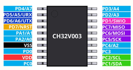
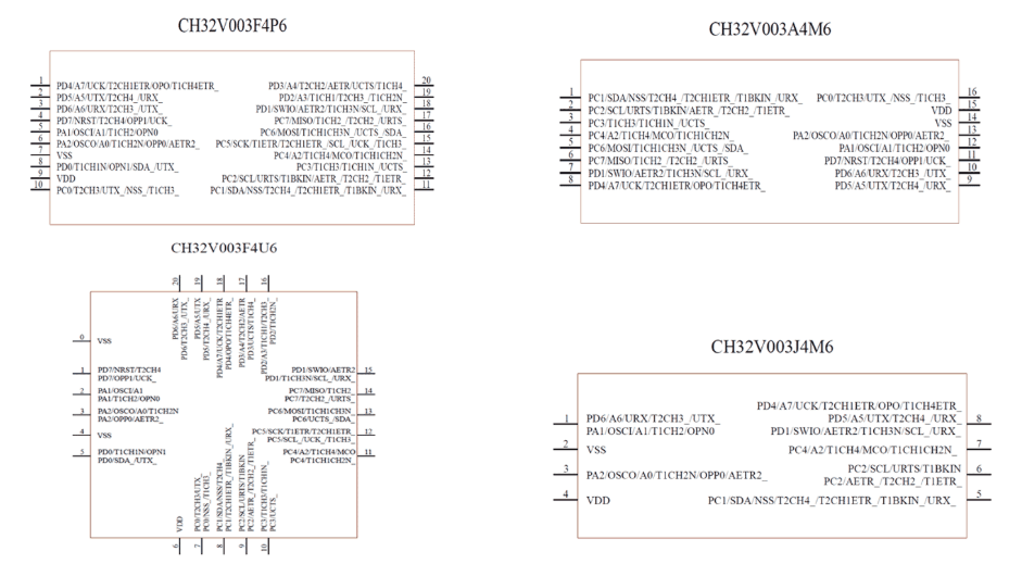
| Pin Name | Alternate Functions | Description |
| PD4 | A7 | GPIO / Analog input |
| PD5 | A5 / URX | GPIO / ADC / UART Receive |
| PD6 | A6 / UTX | GPIO / ADC / UART Transmit |
| PD7 | NRST | Reset pin (active low) |
| PA1 | — | General-purpose I/O |
| PA2 | A0 | GPIO / Analog input |
| VSS | — | Ground |
| PD0 | — | General-purpose I/O |
| VDD | — | Power supply |
| PC0 | — | General-purpose I/O |
| PD3 | A4 | GPIO / Analog input |
| PD2 | A3 | GPIO / Analog input |
| PD1 | SWIO | Debug interface (Single Wire) |
| PC7 | MISO | SPI Master Input Slave Output |
| PC6 | MOSI | SPI Master Output Slave Input |
| PC5 | SCK | SPI Clock |
| PC4 | A2 | GPIO / Analog input |
| PC3 | SCL | I2C Clock |
| PC2 | SCL | I2C Clock (alternate) |
| PC1 | SDA | I2C Data |
• CH32V006
• CH32V103
• GD32VF103
• STM32F030
• STM32F103
• GD32F103
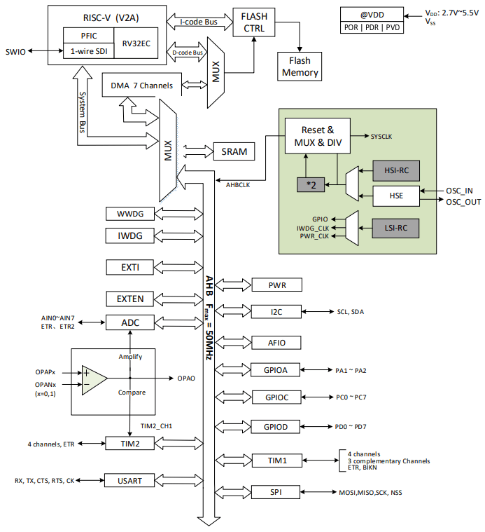
Block diagram of the CH32V003 shows how its internal modules are connected to form a complete microcontroller system. At the core is the RISC-V CPU (RV32EC), which executes instructions and controls all operations. It connects to flash memory through separate instruction and data buses, allowing faster access to stored programs. The flash controller manages reading and writing, while SRAM provides temporary data storage during execution.
The system bus acts as the main communication path, linking the CPU to peripherals such as GPIO, timers, ADC, and communication interfaces. A built-in DMA controller improves efficiency by moving data between modules without heavy CPU involvement. This helps maintain smooth operation when handling multiple tasks.
The clock and reset block controls system timing. It uses internal and external oscillators, along with dividers, to generate the main system clock. Power management and reset circuits ensure stable startup and safe operation.
Peripheral blocks like USART, SPI, I2C, timers, and ADC are connected through the bus, enabling the microcontroller to process signals, communicate, and interact with external hardware through its pins.
| Category | Specification / Feature |
| Core | QingKe 32-bit RISC-V core (RV32EC) |
| Clock Speed | Up to 48 MHz system frequency |
| Interrupt System | Fast interrupt controller, hardware stack, 2-level nesting |
| Flash Memory | 16 KB CodeFlash |
| SRAM | 2 KB data memory |
| Bootloader | 1920 B BootLoader |
| Non-Volatile Memory | 64 B system config + 64 B user-defined |
| Supply Voltage | 3.3V / 5V |
| Low Power Modes | Sleep, Standby |
| Internal Oscillator | 24 MHz RC (factory trimmed), 128 kHz RC |
| External Oscillator | 4–25 MHz (HSE) |
| Reset Features | Power-on reset, power-down reset, voltage detector |
| DMA Controller | 1 controller, 7 channels, supports ring buffer |
| DMA Support | TIM, ADC, USART, I2C, SPI |
| ADC | 10-bit ADC, 0–VDD range, 8 external + 2 internal channels |
| Analog Features | Built-in OPA and comparator |
| Timers | 1×16-bit advanced timer (PWM, brake), 1×16-bit general timer |
| Watchdog Timers | Independent (IWDG) and Window (WWDG) |
| SysTick | 32-bit system timer |
| USART | 1 interface |
| I2C | 1 interface |
| SPI | 1 interface |
| GPIO | 3 ports, up to 18 I/O pins |
| External Interrupts | Supports external interrupt mapping |
| Unique ID | 64-bit unique identifier |
| Debug Interface | 1-wire serial debug (SDI / SWIO) |
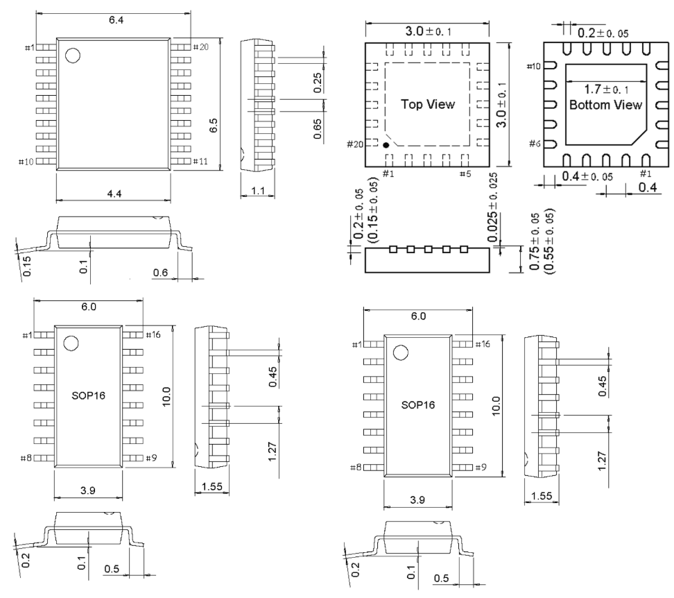
| Package Options | SOP, TSSOP, QFN |
The circuit diagram shows how the CH32V003 operates as a complete microcontroller system with power, clock, reset, and programming connections. The VDD pin is connected to the supply voltage, while a decoupling capacitor (C1) helps stabilize the power and reduce noise. The GND pin provides the reference for the circuit. This ensures the chip receives clean and stable power during operation.
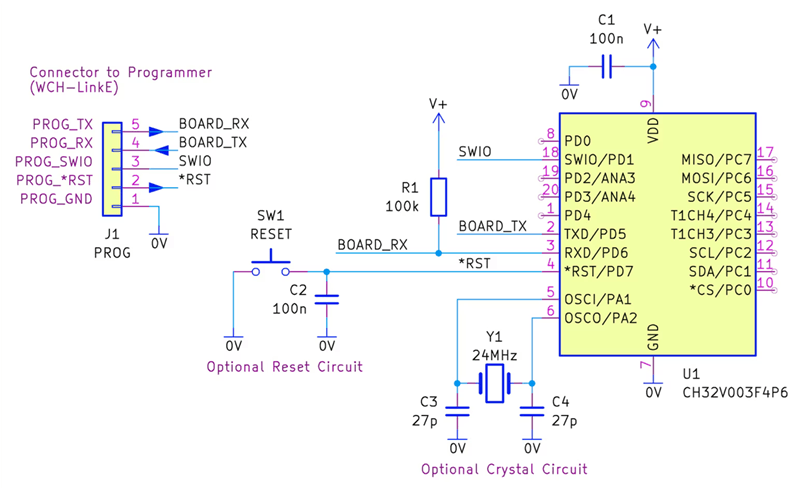
Programming and debugging are handled through the SWIO (single-wire interface) using an external programmer. The PROG connector links signals such as TX, RX, SWIO, RESET, and GND to the microcontroller. This allows firmware to be uploaded and tested without removing the chip from the circuit.
The reset section includes a push button (SW1) and a capacitor (C2), forming a simple reset circuit. When pressed, the reset line is pulled low to restart the microcontroller. A pull-up resistor (R1) keeps the reset line stable during normal operation.
For clock generation, the circuit can use an optional external crystal (Y1) with capacitors (C3 and C4) for improved timing accuracy. If not used, the microcontroller can rely on its internal oscillator. Together, these components allow the CH32V003 to run code, communicate, and control signals through its GPIO and peripheral interfaces.
• Consumer Electronics Control – The CH32V003 is used to manage buttons, simple displays, and basic control logic in small electronic devices.
• Home Automation Modules - Controls switching, timing, and automation tasks in compact smart home circuits.
• Sensor Interface Systems – Reads and processes signals from sensors like temperature or light using its built-in ADC.
• LED and Lighting Control – The CH32V003 generates PWM signals to control LED brightness and lighting patterns.
• Motor Control Circuits – Drives small motors by providing precise PWM outputs for speed control.
• Communication Devices – The CH32V003 handles data exchange between devices through UART, SPI, or I2C interfaces.
The CH32V003 offers strong value by combining a 32-bit RISC-V core with low cost and compact size. It provides sufficient performance for many embedded tasks with a clock speed up to 48 MHz, while keeping power consumption low. The integration of useful peripherals such as ADC, timers, UART, SPI, and I2C reduces the need for external components and simplifies circuit design. It also supports flexible power operation from 3.3V to 5V, making it easy to use in different systems. The built-in DMA, watchdog timers, and debug interface further improve efficiency, reliability, and development convenience.
The CH32V003 has limited memory resources, with only 16 KB of flash and 2 KB of SRAM, which restricts its use in more complex applications. It also has fewer peripherals and interfaces compared to higher-end microcontrollers, which may limit expansion options. The development ecosystem and community support are not as large as more established platforms, which can make learning and troubleshooting more challenging. In addition, it lacks advanced features such as high-speed connectivity or large-scale processing capability, making it less suitable for demanding or data-intensive systems.
The CH32V003 RISC-V core, integrated peripherals, and flexible design make it a strong option for compact embedded systems that require reliable operation without high resource demands. While it has limitations in memory and advanced features, its efficiency and affordability make it a valuable choice for many control and interface tasks.

 FPGA / CPLD
 Memory
 MOS
MOS  MCU
MCU  DSP
DSP OCEP
OCEP Secondary
  Other
Other