
 FPGA / CPLD
 Memory
 MOS
MOS  MCU
MCU  DSP
DSP OCEP
OCEP Secondary
  Other
Other 
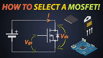
The selection of MOSFETs for DC /DC switching controllers is a difficult task. Selecting the correct MOSFET requires more than just looking at the voltage and current specifications. A compromise between low gate charge and low on-resistance must be established to maintain the MOSFET within specification. The scenario becomes more complicated in a multi-load power system.

Figure.1 Schematic of a step-down synchronous switching regulator
Due to its excellent efficiency, DC/DC switching power supply is widely used in many modern electronic systems. Figure 1 illustrates a step-down synchronous switching regulator with both a high-side and a low-side FET. The two FETs switch according to the controller's duty cycle, with the goal of achieving the desired output voltage. A buck regulator's duty cycle equation is as follows:
1. Duty cycle (high side FET. top tube) = Vout/(Vin*efficiency)
2. Duty cycle (low-side FET. lower tube) = 1 – DC (high-side FET )
One of the simplest solutions is to put the FET into the same chip as the controller, The FET. on the other hand, must be external to the controller at all times in order to give high current capability and/or achieve higher efficiency. Because the FETs are physically isolated from the controller. this allows for optimal heat dissipation and FET selection flexibility. The disadvantage is that the FET selection process is more difficult because of the numerous aspects to consider.
"Why can't this 10A FET also be utilized in my 10A design?" is a popular question. This 10A current rating is not accessible for all designs, according to the answer.
Voltage rating, ambient temperature, switching frequency, controller driving capability, and thermal component area are all factors to consider when choosing a FET, the crucial point is that the FET can overheat and catch fire if the power dissipation is too great and the heat dissipation is insufficient. Using the package/cooling component ThetaJA or thermistor, FET power dissipation, and ambient temperature, we may estimate the junction temperature of a FET as follows:
3. Tj=ThetaJA*FET power consumption (PdissFET) + ambient temperature Tj=ThetaJA*FET power consumption (PdissFET) + ambient temperature (Tambient)
Calculating the FET's power dissipation is required. There are two key components to this power dissipation: AC and DC losses. The following formulae can be used to determine these losses:
4. AC loss: AC power consumption (PswAC) = ½*Vds*Ids*(trise+tfall)/Tsw
where Vds is the high-side FET's input voltage, Ids is the load current, trise and tfall are the FET's rise and fall timings, and Tsw is the controller's switching time (1/switching frequency).
5. DC loss: PswDC=RdsOn*Iout*Iout*duty cycle
The on-resistance of the FET is RdsOn, while the load current of the buck topology is Iout.
Other sources of losses include output parasitic capacitance, gate losses, and body diode losses owing to conduction during the low-side FET's dead time, but we'll concentrate on AC and DC losses in this article.
AC switching losses occur when the switch voltage and current are both non-zero during the switch on and off transition. This is depicted in Figure 2 by the highlighted portion. One strategy to lessen this loss, according to Equation 4, is to shorten the switch's rise and fall durations. This can be accomplished by selecting a FET with a lower gate charge. The switching frequency is also a factor. Figure 3 shows the percentage of switching time spent in the rise and fall transition region as a function of switching frequency. As a result, higher frequencies result in higher AC switching losses. Reduce the switching frequency to reduce AC losses, however, this necessitates a larger and typically more expensive inductor to keep the peak switch current within specification.

Figure.2 AC loss graph

Figure.3 Effect of switching frequency on AC losses
The DC loss happens when the switch is turned on due to the FET's on-resistance. As demonstrated in Figure 4, this is a fairly simple I2R loss formation mechanism. On-resistance, on the other hand, changes with FET junction temperature, complicating the situation. As a result, an iterative method must be utilized to precisely compute the on-resistance when applying equations 3), 4), and 5 while taking into account the temperature rise of the FET, choosing a low on-resistance FET is one of the simplest techniques to reduce DC losses. Furthermore, as previously stated, the magnitude of the DC losses is related to the percent on-time of the FET. which is the high-side FET controller duty cycle plus 1 minus the low-side FET duty cycle. We may deduce from Figure 5 that longer on-time equates to higher DC switching losses; thus, DC losses can be decreased by lowering the on-time/FET duty cycle. For instance, if an intermediate DC rail is utilized and the input voltage can be changed, the duty cycle can be changed.

Figure.4 DC loss graph

Figure.5 The effect of duty cycle on DC losses
While selecting a FET with a low gate charge and low on-resistance is a simple option, there are certain tradeoffs and tradeoffs between these two factors. Low gate charge usually translates to a smaller gate area/fewer parallel transistors, and hence a higher on-resistance. Using larger/more parallel transistors, on the other hand, often results in lower on-resistance and hence higher gate charge. This means that FET selection must strike a balance between these two opposing requirements. In addition, the cost factor must be taken into account.
Low-duty-cycle designs require a high input voltage, and the high-side FET is turned off most of the time, resulting in low DC losses. Substantial FET voltages, on the other hand, result in high AC losses, hence FETs with low gate charge, even with high on-resistance, can be chosen. The low-side FET is active for the majority of the time, although it has very low AC losses. Because of the FET body diode, the voltage of the low-side FET during on/off is quite low. As a result, a FET with a low on-resistance must be chosen, and the gate charge might be high. Figure 7 depicts the circumstances described previously.

Figure.6 High-side and low-side FET power dissipation for low duty cycle designs
We can have a high duty cycle design with the high-side FET on most of the time if we lower the input voltage, as illustrated in Figure 7. The DC losses are considered in this scenario, hence a low on-resistance is required. AC losses may not be as significant as with low-side FETs depending on the input voltage, but they are still not as low. As a result, a low gate charge is still necessary. This necessitates striking a balance between low on-resistance and low gate charge. We can choose the proper FET based on price or size rather than on-resistance and gate charge because low-side FETs have the shortest on-time and low AC losses.

Figure.7 High-side and low-side FET power dissipation for high duty cycle designs
What is the optimal solution, high input voltage/low duty cycle, or low input voltage/high duty cycle, assuming a point-of-load (POL) regulator with a rated input voltage of some intermediate voltage rail? What about the empty-to-occupied ratio? Modulate the duty cycle while watching FET power dissipation using varied input voltages.
The high-side FET response plot in Figure 8 indicates that as the duty cycle increases from 25% to 40%, the AC losses reduce dramatically while the DC losses grow linearly. As a result, when selecting a capacitor and on-resistance balance FET, a duty cycle of roughly 35 percent should be optimum. We can employ a low on-resistance FET and trade-off high gate charge by continuously lowering the input voltage and increasing the duty cycle, which results in the lowest AC losses and largest DC losses. DC losses drop linearly as the controller duty cycle increases from low (low-side FET on-time is shorter), with minimum losses at high controller duty cycles, as shown in Figure 9. Because AC losses are low across the board, FETs with low on-resistance should be used in any circumstance.

Figure.8 High-side FET losses versus duty cycle

Figure.9 Low-side FET losses versus controller duty cycle
Note: The low-side FET duty cycle is 1 - controller duty cycle, so the low-side FET on-time decreases as the controller duty cycle increases.
Figure 10 depicts how the total efficiency changes when high- and low-side losses are combined. We can observe that at high duty cycles, the combined FET losses are lowest and the efficiency is maximum. From 94.5 percent to 96.5 percent, efficiency improved. Unfortunately, because the mid-rail supply is driven from a fixed input supply, we must lower its voltage to achieve a low input voltage, which increases its duty cycle. As a result, some or all of the gains obtained at the POL may be canceled. Another option is to bypass the intermediate rail and proceed straight from the input supply to the POL regulator, hence minimizing the number of regulators.

Figure.10 Total loss versus efficiency and duty cycle
In power systems with multiple output voltage and current needs, the problem becomes more complicated. Different POL regulator duty cycles are compared for efficiency, cost, and size. Figure 11 depicts a system with a 28V input voltage and a total of 8 loads varying in voltage from 3.3V to 1.25V. There are three methods of comparison: 1) To obtain a low duty cycle of the POL regulator, feed 28V directly through the input power supply; 2) Use 12V intermediate rail, medium duty cycle of POL regulator; 3) Use 5V mid rail, high duty cycle of POL regulator. The comparison findings are shown in Figure 12. The architecture without a mid-rail supply has the lowest cost, the 12V mid-rail voltage architecture has the maximum efficiency, and the 5V mid-rail voltage architecture has the smallest volume in this situation. As a result, we can observe that there is no apparent trend in any of these metrics for this huge system that we see with a single POL supply. This is because, in addition to the mid-rail regulator, each regulator has separate load current and voltage requirements that can conflict with one another when many regulators are utilized. The easiest method to analyze this scenario is to evaluate the various choices using a tool like WEBENCH Power Designer.
 supply, and load.jpg")
Figure.11 Power system showing input, mid-rail, point-of-load (POL) supply, and load
The different middle rail voltage options are 28V (using the input power directly), 12V, and 5V. As a result, the POL regulator's duty cycle changes.

Figure.12 Power supply design graph showing the effect of mid-rail voltage on power system efficiency, size, and cost.
